A method of preparation of an epitaxial substrate
一种基片、外延的技术,应用在外延基片的制备领域,能够解决高生产成本、负面影响无法排除等问题
- Summary
- Abstract
- Description
- Claims
- Application Information
AI Technical Summary
Problems solved by technology
Method used
Image

Examples
Embodiment Construction
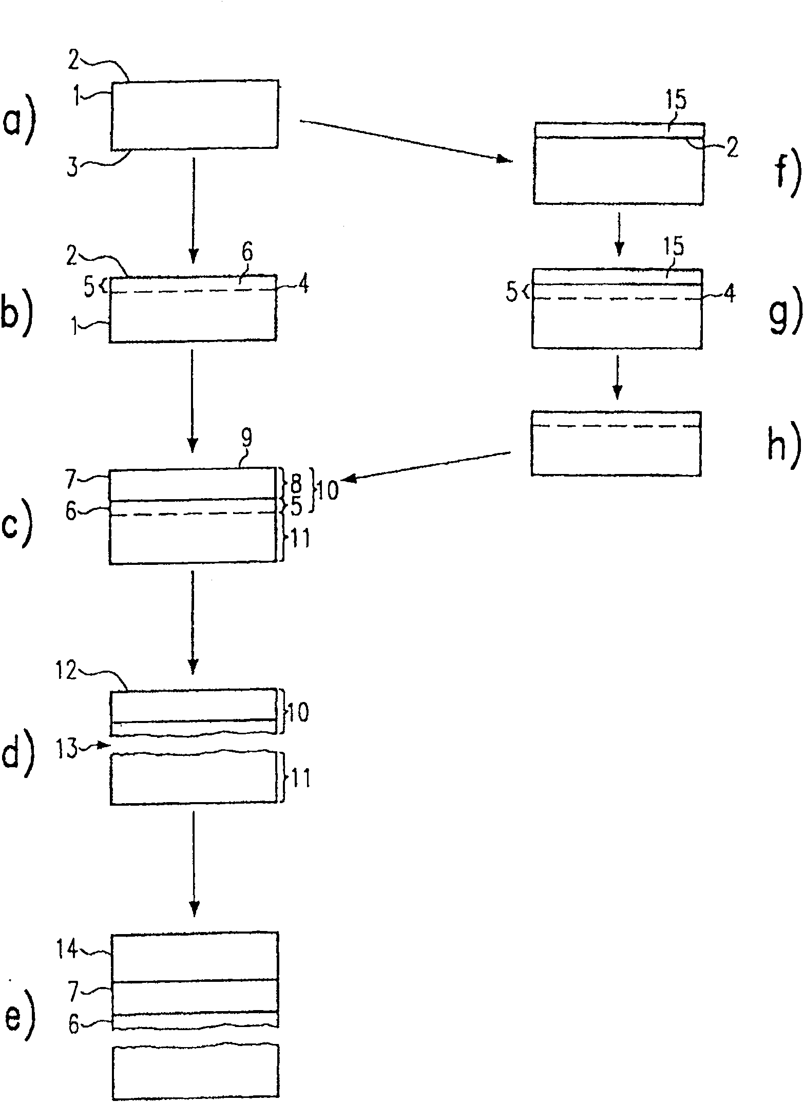
[0043] figure 1 a shows the underlying substrate as the starting point of the epitaxial substrate fabrication process. The substrate 1 has a front side 2 and a back side 3 . For homoepitaxial or heteroepitaxial applications, the underlying substrate is usually crystalline, especially of the single crystal type. At least one surface (here the front side 2 ) is sufficiently well-defined as a starting point for epitaxial (homoepitaxial or heteroepitaxial) layer or film growth. Typically, the surface is polished and prepared for epitaxy, and is essentially aligned with the usual crystallographic orientation. The exact dimensions of the underlying substrate 1 are not critical in importance, but at least the surface of the front side 2 should be large enough to allow the growth of an epitaxial substrate large enough for subsequent device needs. Of particular relevance are wafers made of silicon, silicon carbide, sapphire, gallium arsenide, indium phosphide or germanium. These wa...
PUM
| Property | Measurement | Unit |
|---|---|---|
| diameter | aaaaa | aaaaa |
Abstract
Description
Claims
Application Information
 - R&D
- Intellectual Property
- Life Sciences
- Materials
- Tech Scout
- Unparalleled Data Quality
- Higher Quality Content
- 60% Fewer Hallucinations
Browse by: Latest US Patents, China's latest patents, Technical Efficacy Thesaurus, Application Domain, Technology Topic, Popular Technical Reports.
© 2025 PatSnap. All rights reserved.Legal|Privacy policy|Modern Slavery Act Transparency Statement|Sitemap|About US| Contact US: help@patsnap.com