Optoelectronic component

A technology of optoelectronic devices and chips, which is applied in the direction of electric solid devices, electrical components, semiconductor devices, etc., can solve problems such as defective contrast, achieve good contrast, and reduce disturbing reflections

Inactive Publication Date: 2010-02-03
OSRAM OPTO SEMICON GMBH & CO OHG
View PDF7 Cites 3 Cited by
  • Summary
  • Abstract
  • Description
  • Claims
  • Application Information

AI Technical Summary

Problems solved by technology

In addition, when incident ambient light is incident, defective contrasts result from ambient light reflected on the emission surface and chip surface.

Method used


Image

  • Optoelectronic component
  • Optoelectronic component
  • Optoelectronic component

Examples


Embodiment Construction

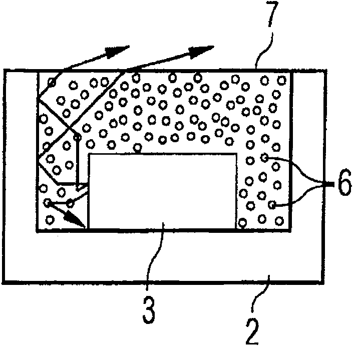
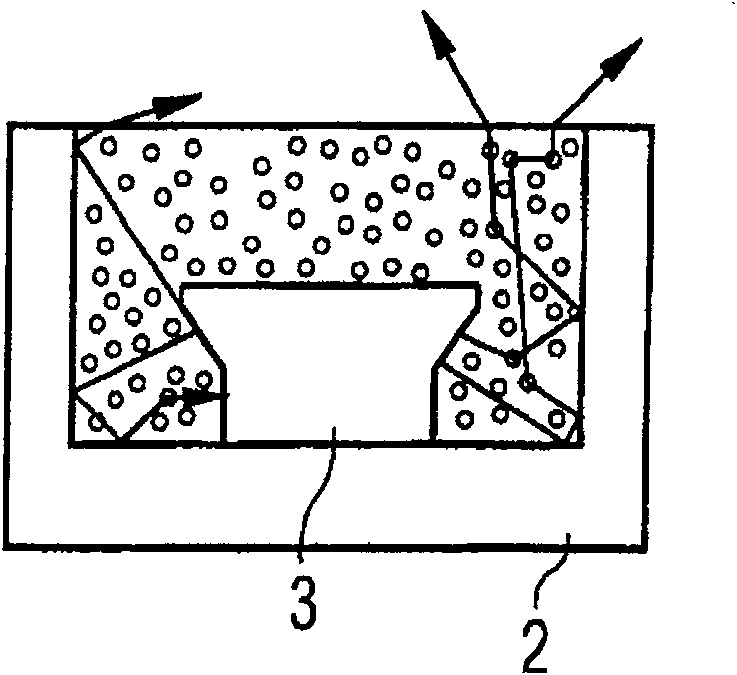
[0044] first with the help of figure 1 The basic construction of the optoelectronic device according to the invention will be explained. The different possible embodiments of the component are then described with reference to FIGS. 2 and 3 , as well as the mode of operation according to the invention. Finally, three test series were carried out by the inventors, the measurement results of which are shown by means of FIGS. 4-11 .

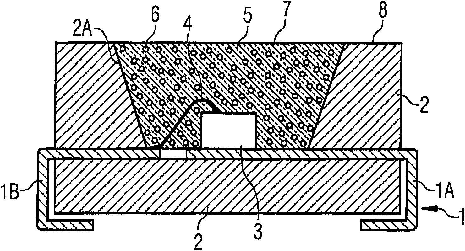
[0045] figure 1 A schematic cross-sectional view of a surface-mountable optoelectronic component constructed according to the invention is shown in . The base body 2 is formed under housing molding conditions by injecting the leadframe 1 from the outside with a suitable plastic material. The housing has a central recess in which a semiconductor chip 3 , for example an optoelectronic transmitter chip, is arranged and electrically conductively connected to the electrical connections 1A, 1B of the lead frame 1 by means of wire bonding 4 .

[0046]...


PUM


Abstract

Optoelectronic component, having a basic body or housing ( 2 ), at least one optoelectronic semiconductor chip ( 3 ) arranged in a recess of the basic body, and a potting composition ( 5 ) made of a transparent material, which potting composition embeds the at least one semiconductor chip in the recess, the transparent potting composition ( 5 ) being formed in diffusely scattering fashion and in particular containing diffuser particles ( 6 ) at which light impinging thereon is diffusely scattered.

Description

technical field [0001] The invention relates to an optoelectronic device, in particular to a surface mountable optoelectronic device. Background technique [0002] In conventional surface-mountable optoelectronic components, the precased component is first produced in such a way that a prefabricated lead frame is injected with a suitable synthetic material which forms the housing of the component. The component has, for example, a recess or a cutout on the upper side, into which lead frame connections are introduced from opposite sides, wherein a semiconductor chip, for example a LED chip, is bonded and electrically connected to a connection connected. The gap is then filled with clear, translucent potting compound. For example from the literature This basic form of a surface mountable optoelectronic device is disclosed in "Siemens SMT Top LEDs for Surface Mounting (TOPLED)" by G. Waitl, Siemens Components 29 (1991), No. 4, pp. 147-149. [0003] In these known surface-m...

Claims


Application Information

Patent Timeline
Patent Type & Authority Patents(China)
IPC IPC(8): H01L33/00H01L25/075H01L33/56
CPCH01L2933/0091H01L2224/48091H01L2224/48247H01L2224/48465H01L25/0753H01L2924/3025H01L33/56H01L2924/00014H01L2924/00
Inventor K·阿恩德特N·法希特奇安
Owner OSRAM OPTO SEMICON GMBH & CO OHG
Why Eureka
Try Eureka