Ceramic substrate

A ceramic substrate, ceramic thin plate technology, applied in printed circuit components, electrical components, printed circuits, etc., can solve the problem of large-scale ceramic substrates, and achieve the effect of reducing material costs

Inactive Publication Date: 2007-08-15
ALPS ALPINE CO LTD
View PDF0 Cites 3 Cited by
  • Summary
  • Abstract
  • Description
  • Claims
  • Application Information

AI Technical Summary

Problems solved by technology

[0010] Therefore, in the first and second structures, there is a large aperture of the hole 53 between the lamination layers. When forming a wiring pattern between the lamination layers, it is necessary to arrange the wiring pattern in a state avoiding the large aperture. Therefore, there is a The problem of increasing the size of the ceramic substrate

Method used


Image

  • Ceramic substrate
  • Ceramic substrate

Examples


Embodiment Construction

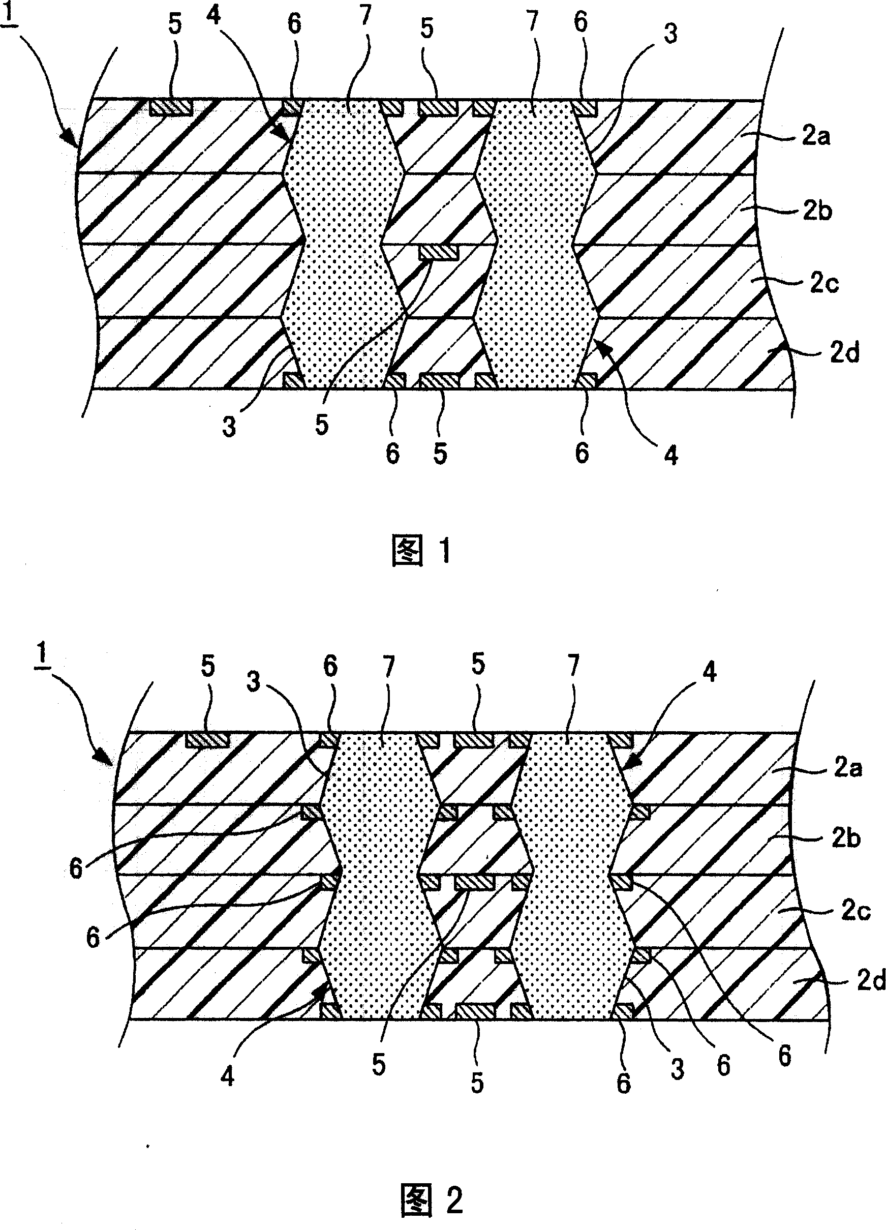
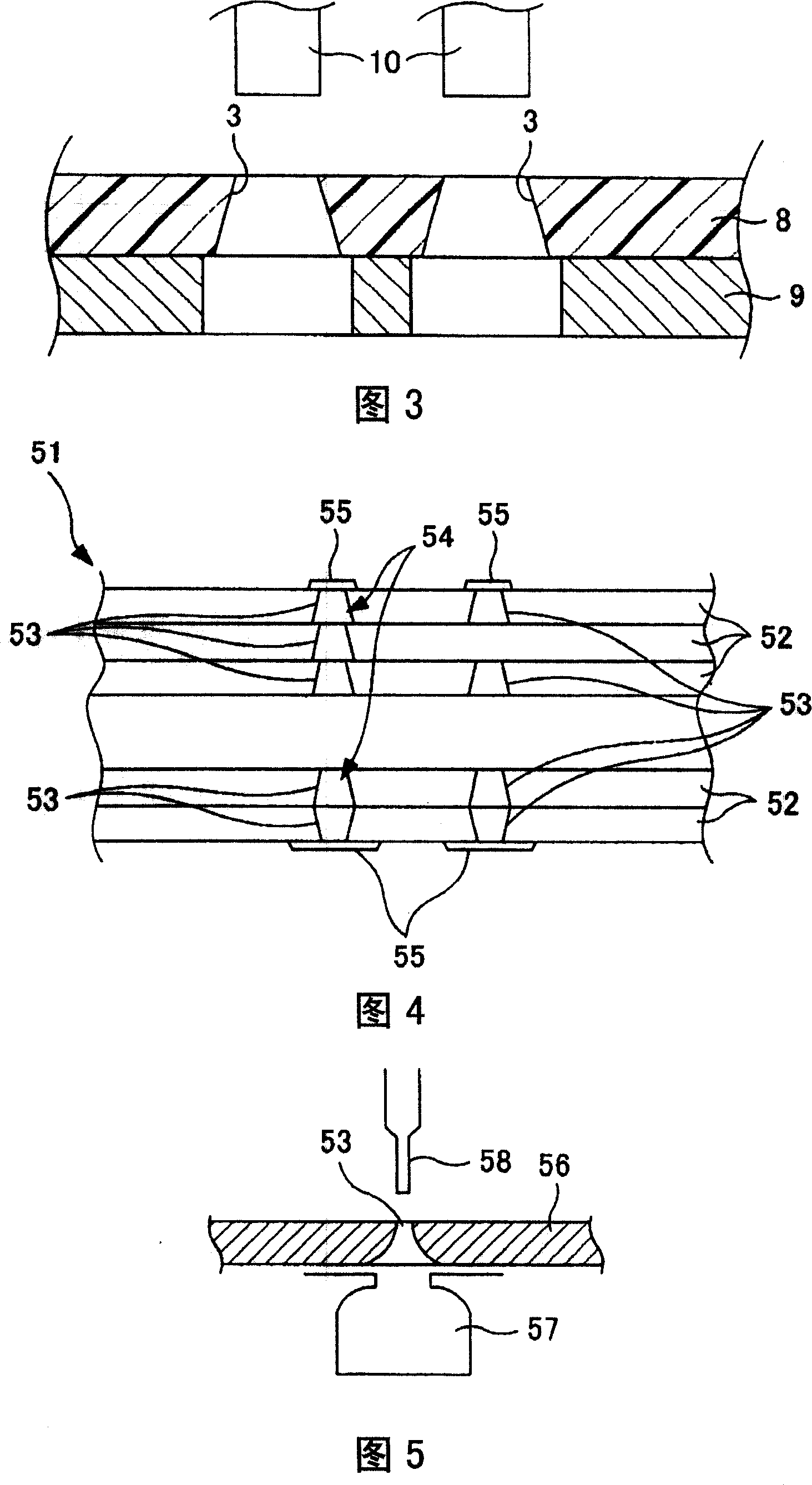
[0030] Hereinafter, embodiments of the present invention will be described with reference to the accompanying drawings. FIG. 1 is a sectional view of main parts of a first embodiment of a ceramic substrate of the present invention, and FIG. 2 is a sectional view of main parts of a second embodiment of a ceramic substrate of the present invention. , FIG. 3 is an explanatory view showing a method of manufacturing a ceramic substrate of the present invention.

[0031] Next, the structure of the first embodiment of the ceramic substrate of the present invention will be described with reference to FIG. 1. The ceramic substrate 1 is made of low-temperature co-fired ceramics (LTCC) or the like, for example, by laminating a plurality of (four) ceramic thin plates 2a to 2d. And formed.

[0032] The ceramic thin plates 2a-2d are provided with holes 3 formed in the shape of a cone, and the holes 3 are connected to each other in the vertical direction to form a through hole (a state in wh...


PUM


Abstract

The invention provides a compacted ceramic substrate. It escapes the small aperture state to form wiring pattern when the wiring pattern is formed in the lamination with the connection of the small aperture. It obtains densification of the wiring pattern in the lamination and miniaturization of the ceramic wafer so as to get a cheap ceramic wafer.

Description

technical field [0001] The present invention relates to an effective ceramic substrate used in various electronic devices, electronic circuit units, and the like. Background technique [0002] At first existing ceramic substrate view is described, and Fig. 4 is the cross-sectional view of main part of existing ceramic substrate, and Fig. 5 is the explanatory drawing that shows the manufacturing method of existing ceramic substrate, below, in conjunction with Fig. 4 the existing The structure of the ceramic substrate will be described, and the ceramic substrate 51 is formed by laminating a plurality of ceramic thin plates 52 . [0003] The ceramic thin plate 52 is provided with a hole 53 formed into a truncated cone. As shown in the upper part (first structure) of FIG. It is formed so that a plurality of holes 53 are connected to each other in the vertical direction (the holes 53 are arranged in the same direction), thereby constituting a through hole (via) 54. In addition, ...

Claims


Application Information

Patent Timeline
IPC IPC(8): H05K1/02H05K1/00
Inventor 山本耕平滨野雅章
Owner ALPS ALPINE CO LTD
Why Eureka
Try Eureka