camera device

A technology for an imaging device and a solid-state imaging element, which is applied in radiation control devices, image communication, television, etc., can solve the problems of complex manufacturing process, degradation of pixel array image quality, and poor yield.

Active Publication Date: 2016-08-10
NIKON CORP
View PDF7 Cites 0 Cited by
  • Summary
  • Abstract
  • Description
  • Claims
  • Application Information

AI Technical Summary

Problems solved by technology

Therefore, the manufacturing process becomes complicated and the yield becomes poor
In addition, during high-speed operation, the heat generated by the chip, especially the heat generated by the A / D converter, increases, and there is a possibility that the pixel array may be adversely affected by a decrease in image quality due to temperature rise.

Method used


Image

  • camera device
  • camera device
  • camera device

Examples


Embodiment Construction

[0030] Next, an imaging device according to an embodiment of the present invention will be described with reference to the drawings.

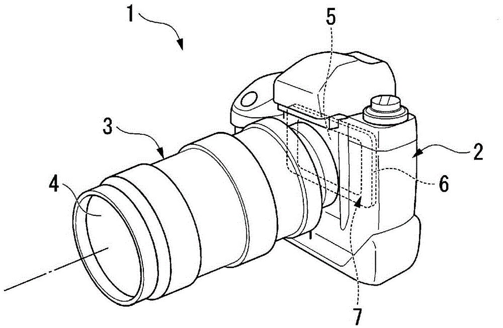
[0031] figure 1 The imaging device 1 of this embodiment is shown. The imaging device 1 is a so-called digital single-lens reflex camera. In the imaging device 1, a lens barrel 3 is detachably mounted on a lens holder (not shown) of a camera body 2, and light passing through a lens 4 of the lens barrel 3 is disposed on the camera body 2. The image is formed on the sensor chip (solid-state image sensor) 5 of the multi-chip module 7 on the back side. The sensor chip 5 is a so-called bare chip of a CMOS image sensor or the like.

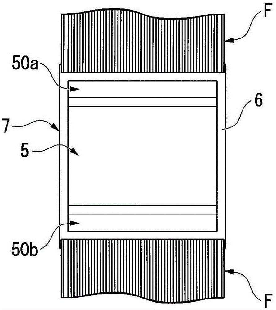
[0032] Such as figure 2 As shown, the multi-chip module 7 includes a sensor chip 5, an upper signal processing chip 50a, and a lower signal processing chip 50b.

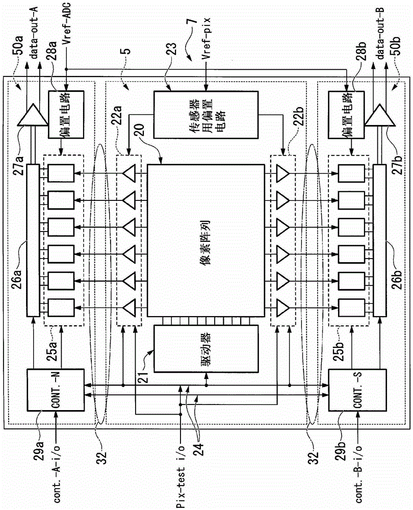
[0033] The sensor chip 5 includes: a pixel array 20, which is composed of a plurality of pixels that output signals corresponding to incident light (herei...


PUM


Abstract

The imaging device includes a solid-state imaging element and a substrate. The solid-state imaging device has a pixel array in which a plurality of pixels are arranged in a two-dimensional matrix, and pads ( 51 ) provided corresponding to pixel columns of the pixel array and outputting signals of pixels in the pixel column. A signal output terminal group having a plurality of pads (51) arranged in a line along the column direction of the pixel array is arranged along the row direction of the pixel array. The substrate ( 6 ) has laminated wiring for each signal output terminal group, and the laminated wiring is formed by stacking a plurality of wiring layers extending in the column direction of the pixel array. The laminated wiring (32) includes a first terminal portion (61) provided at a position facing each pad (51) of the signal output terminal group. The pad (51) is connected to the first terminal portion (61) via the pad (9).

Description

technical field [0001] The present invention relates to an imaging device for capturing an image of a subject. [0002] this application claims priority based on Japanese Patent Application No. 2010-251980 for which it applied on November 10, 2010, and uses the content here. Background technique [0003] In recent years, higher-speed operation is required for large-scale sensor chips used in so-called digital single-lens reflex cameras and the like. By providing an A / D converter for each column of the pixel array provided on this chip and performing signal processing in parallel, the processing speed of the A / D converter is kept relatively low, and low power consumption is realized. However, when high-speed processing is achieved, a sensor unit with low noise, a large dynamic range, and a high power supply voltage, and a digital circuit equipped with tiny transistors and operating at ultra-high speed with a low power supply voltage are composed of a single chip. Therefore,...

Claims


Application Information

Patent Timeline
Patent Type & Authority Patents(China)
IPC IPC(8): H01L27/146H01L27/14H04N5/369
CPCH01L27/14618H01L2924/0002H01L2924/00H04N25/00
Inventor 末延一彦
Owner NIKON CORP
Why Eureka
Try Eureka