Liquid crystal display device, and driving circuit and driving method used in same

A technology of liquid crystal display device and driving circuit, which can be used in static indicators, nonlinear optics, instruments, etc., and can solve problems such as unsolvable problems.

Inactive Publication Date: 2007-08-29
NEC LCD TECH CORP
View PDF5 Cites 4 Cited by
  • Summary
  • Abstract
  • Description
  • Claims
  • Application Information

AI Technical Summary

Problems solved by technology

However, the above problems cannot be solved

Method used


Image

  • Liquid crystal display device, and driving circuit and driving method used in same
  • Liquid crystal display device, and driving circuit and driving method used in same
  • Liquid crystal display device, and driving circuit and driving method used in same

Examples


no. 1 example

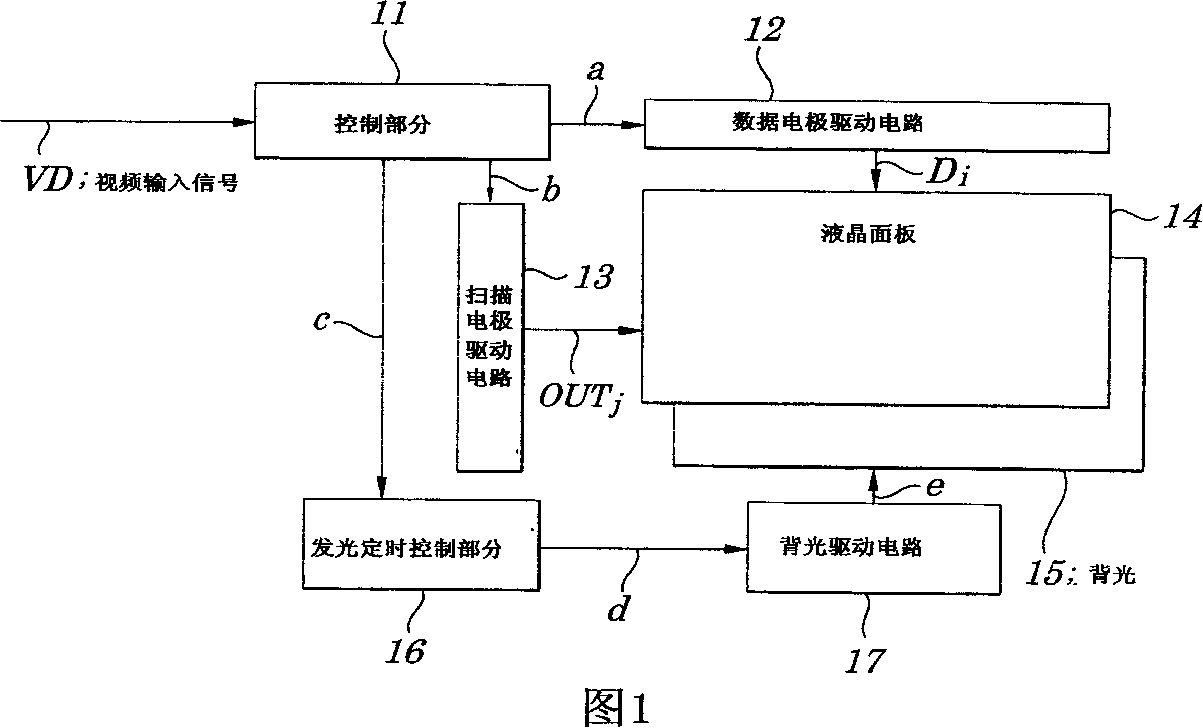
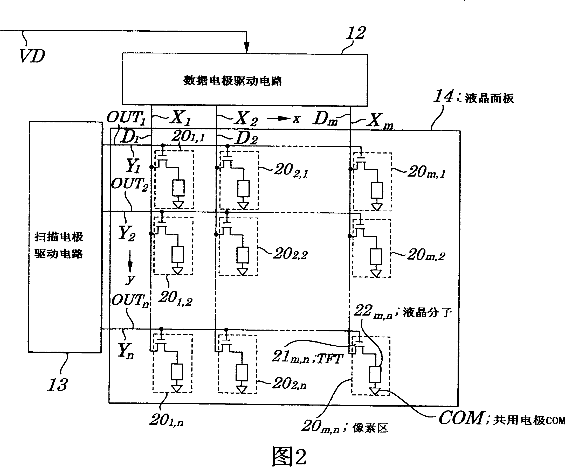
[0076] 1 is a block diagram showing the electrical configuration of main parts of a liquid crystal display device according to a first embodiment of the present invention. As shown in FIG. 1, the liquid crystal display device according to the first embodiment of the present invention includes a control section 11, a data electrode drive circuit 12, a scan electrode drive circuit 13, a liquid crystal panel 14, a backlight 15, a light emission timing control section 16 and a backlight drive Circuit 17. FIG. 2 is a circuit diagram showing an example of an electrical structure of the liquid crystal panel of FIG. 1. Referring to FIG. As shown in FIG. 2, the liquid crystal panel 14 includes data electrodes X i (i=1, 2,..., m, for example, m=640×3), scan electrode Y j (j=1, 2, ..., n, for example, m=512), and pixel area (unit) 20 i·j .

[0077] Each data electrode X iare formed at predetermined intervals in the X direction (that is, in the first direction), each of which is supp...

no. 2 example

[0088] FIG. 5 is a block diagram showing the electrical configuration of main parts of a liquid crystal display device according to a second embodiment of the present invention. Each part of the liquid crystal display device shown in FIG. 5 is provided with the same reference numeral as the corresponding part in FIG. 1 . In the liquid crystal display device, as shown in FIG. 5 , instead of data electrode driving circuit 12 and light emission timing control portion 16 shown in FIG. 1 , data electrode driving circuit 12A and light emission timing control portion 16A are provided. The functions of data electrode drive circuit 12A and light emission timing control section 16A are different from those of data electrode drive circuit 12 and light emission timing control section 16 . Data electrode drive circuit 12A converts display signal D corresponding to video input signal "VD" in dot-sequence based on control signal "a" supplied from control section 11. i Each data electrode X ...


PUM


Abstract

A liquid crystal display device is provided which is capable of improving display quality of moving images. In the liquid crystal display device, every time a driving pulse voltage is generated by a backlight driving circuit in synchronization with a timing signal fed from a lighting timing control section and is applied to a backlight and a scanning signal is applied to each scanning electrode of a liquid crystal panel, the backlight is turned OFF during a period before completion of a response of each liquid crystal molecule to application of a display signal and is turned ON at time of the completion of the response. When displacement of each of the liquid crystal molecules is large and therefore the change in light transmittance is large, the backlight is turned OFF and, therefore, no change in luminance on a display screen occurs, as a result, contrast of images can be improved.

Description

technical field [0001] The present invention relates to a liquid crystal display device, a driving circuit and a driving method for the liquid crystal display device, and in particular to a liquid crystal display device which can be suitably used when displaying moving images, and to a driving circuit which can be used for the liquid crystal display device circuit and drive method. [0002] This application claims priority from Japanese Patent Application No. 2006-024416 filed on February 1, 2006, which is hereby incorporated by reference. Background technique [0003] Liquid crystal display devices are generally driven in a holding-type mode in which a current frame is held until display data corresponding to a next frame is supplied. In this case, no problem occurs in devices mainly for displaying still images such as personal computers and the like. However, in the case of a display device such as a liquid crystal television that displays moving images, subsequent image...

Claims


Application Information

Patent Timeline
Patent Type & Authority Applications(China)
IPC IPC(8): G09G3/36G09G3/34G09G3/20G02F1/133G02F1/13357G02F1/1335
CPCG09G2360/145G09G3/3648G09G2320/0257G09G2320/0252G09G3/3406G09G2320/0261G09G2320/0633
Inventor 高桥美朝
Owner NEC LCD TECH CORP
Why Eureka
Try Eureka