Redundancy-function-equipped semiconductor memory device made from ecc memory

A memory and semiconductor technology, applied in static memory, instrumentation, error detection/correction, etc., can solve problems such as intolerable design step design time, reduced operation speed, and slowed down operation speed

Inactive Publication Date: 2007-09-26
FUJITSU MICROELECTRONICS LTD
View PDF3 Cites 25 Cited by
  • Summary
  • Abstract
  • Description
  • Claims
  • Application Information

AI Technical Summary

Problems solved by technology

This brings about the following problems: the operation speed becomes slower and more power consumption is required
Depending on user needs, there may be cases where high-speed memory operation is performed using a redundancy function capable of high-speed operation as a defect repair function in place of the ECC function that causes a decrease in operation speed
However, in this case, if the built-in ECC memory already embedded in the system is modified to a memory with a redundant function by some design change, an intolerably large number of design steps and a large amount of design time are required

Method used


Image

  • Redundancy-function-equipped semiconductor memory device made from ecc memory
  • Redundancy-function-equipped semiconductor memory device made from ecc memory
  • Redundancy-function-equipped semiconductor memory device made from ecc memory

Examples


Embodiment Construction

[0038] Embodiments of the present invention will be described below with reference to the drawings.

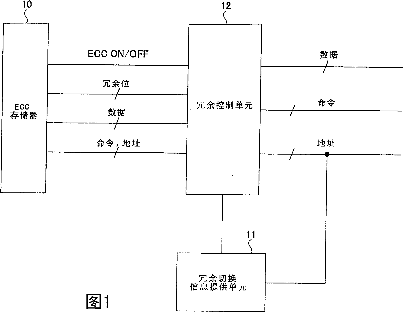
[0039] FIG. 1 is a block diagram showing the configuration of a semiconductor memory device with a redundancy function according to the present invention. The semiconductor memory device with redundancy function of FIG. 1 includes an ECC memory 10 , a redundancy switching information providing unit 11 and a redundancy control unit 12 .

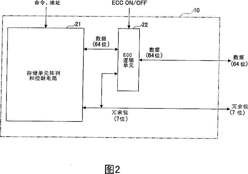
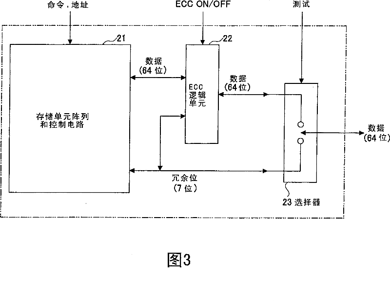
[0040] The ECC memory 10 is a memory block having an error correction function realized using Hamming codes, extended Hamming codes, horizontal and vertical parity codes, and the like. The ECC memory 10 has terminals for inputting commands and addresses, terminals for inputting / outputting data and redundant bits for error correction purposes, and terminals for inputting on / off states indicating the ECC function. Terminal for ECCon / off signal.

[0041] The redundancy control unit 12 is located between the ECC memory 10 and a host device (such...


PUM


Abstract

A semiconductor memory device includes a memory configured to input / output first data and second data in parallel, the first data being all or part of a predetermined number of bits, and the second data being comprised of a number of bits necessary to correct error of the predetermined number of bits, a unit configured to supply redundancy switching information in response to an address signal supplied to the memory, and a controlling unit situated between the memory and input / output nodes, having a first path that couples a given bit of the input / output nodes to a corresponding bit of the first data of the memory and a second path that couples the given bit of the input / output nodes to a predetermined bit of the second data of the memory, and configured to select and enable one of the first path and the second path in response to the redundancy switching information.

Description

technical field [0001] The present invention relates generally to semiconductor memory devices, and more particularly to semiconductor memory devices with redundancy. Background technique [0002] For semiconductor memory devices, methods for repairing errors include a redundancy method using spare memory cells and a data correction method using error correction codes (ECC). [0003] In a semiconductor memory device having a redundancy function, when there is a defective memory cell, such a cell is replaced with a redundant memory cell serving as a spare memory cell, and access to the address of the defective memory cell is directed to the redundant memory cell. The remaining memory cells, so that the address of the defective memory cell can be used. In order to replace a defective memory cell with a redundant memory cell, the address of the defective memory cell needs to be recorded. In a typical redundant system, a fuse is provided and the state of the fuse (broken or in...

Claims


Application Information

Patent Timeline
Patent Type & Authority Applications(China)
IPC IPC(8): G11C29/00G11C29/24
CPCG11C29/42G06F11/1008G11C29/846G11C29/02G11C29/00
Inventor 江渡聪
Owner FUJITSU MICROELECTRONICS LTD
Why Eureka
Try Eureka