Seat structure of diode illuminating device and method for manufacturing diode illuminating device

A light-emitting device and manufacturing method technology, applied in the direction of semiconductor devices, electric solid-state devices, electrical components, etc., can solve the problems of complicated process, poor heat dissipation efficiency, and increased heat dissipation area of ​​the light-emitting diode packaging structure, and achieve high temperature resistance and increase The effect of increasing heat capacity, heat conduction area, and package reliability of components

Inactive Publication Date: 2007-09-26
TOP CRYSTAL TECH
View PDF1 Cites 7 Cited by
  • Summary
  • Abstract
  • Description
  • Claims
  • Application Information

AI Technical Summary

Problems solved by technology

[0005] The technical problem to be solved by the present invention is to provide a base structure of a diode light-emitting device, which can improve the problem of poor heat dissipation and complicated process of the existing plastic-based light-emitting diode packaging structure. The plastic insulator is coated to make it more firmly combined with the heat-conducting body, and the body of the diode light-emitting device is changed to a metal material with good heat conduction to make it. The metal is used as the heat-conducting body, which has high temperature resistance and good heat dissipation. The increase in packaging reliability will greatly increase the heat dissipation area of ​​the light emitting diode packaging structure, thereby enabling the diode chip of the diode light emitting device to obtain better heat dissipation effect when it is working, or it can also make the diode light emitting device of the present invention applicable For higher power product specifications

Method used


Image

  • Seat structure of diode illuminating device and method for manufacturing diode illuminating device
  • Seat structure of diode illuminating device and method for manufacturing diode illuminating device
  • Seat structure of diode illuminating device and method for manufacturing diode illuminating device

Examples


Embodiment Construction

[0053] In order to have a further understanding of the purpose of the present invention, structural features and functions thereof, the relevant embodiments and accompanying drawings are described in detail as follows:

[0054]

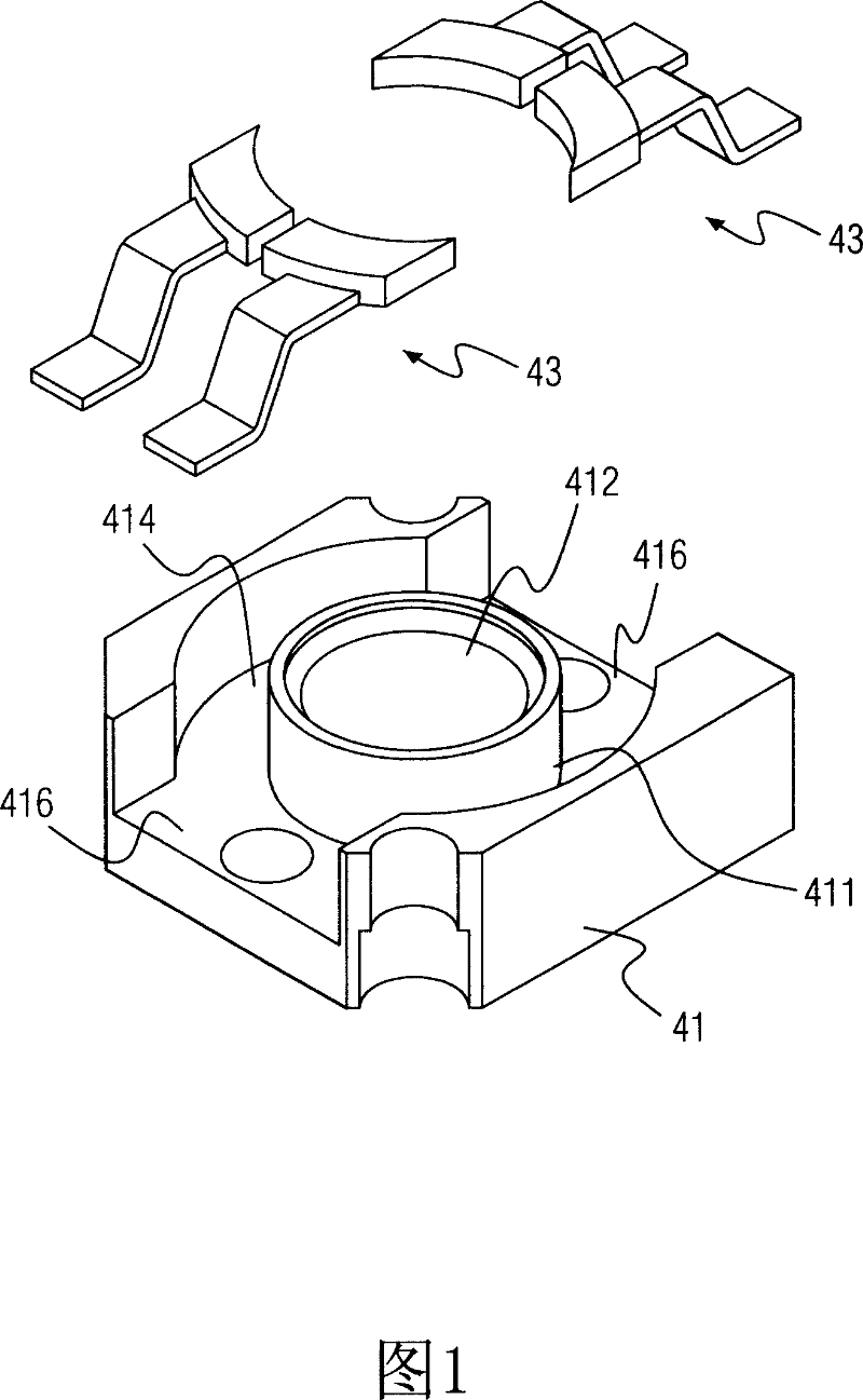
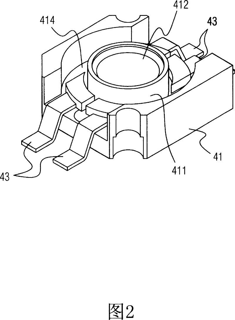
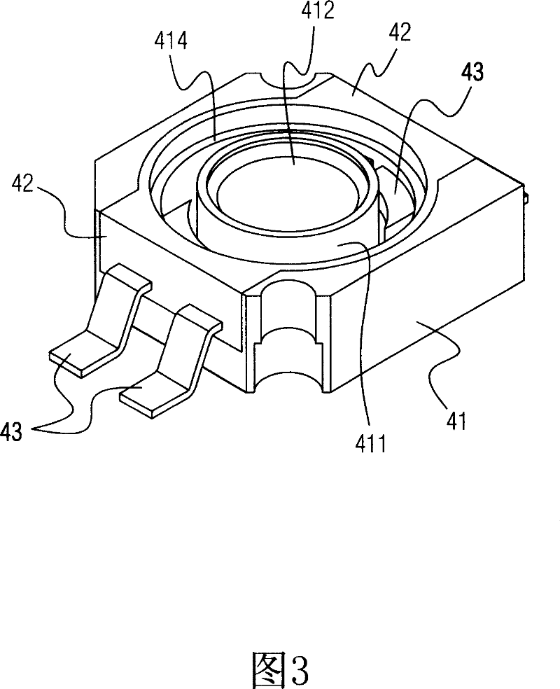
[0055] As shown in FIG. 1 , it is a three-dimensional exploded embodiment diagram of a heat conducting body 41 and a lead frame 43 with a first injection hole 417 but no second injection hole 418 according to the present invention. As shown in FIG. 2 , it is a diagram of an embodiment of the three-dimensional combination of the heat conducting body 41 with the first injection hole 417 but without the second injection hole 418 and the lead frame 43 of the present invention. As shown in FIG. 3 , it is a three-dimensional combination embodiment diagram of a heat conducting body 41 , a lead frame 43 and a plastic insulator 42 with a first injection hole 417 but without a second injection hole 418 according to the present invention. As shown in FIG. 4 , ...


PUM


Abstract

The invention discloses a seat structure and manufacturing method of diode irradiance device, thereinto the irradiance device includes seat structure, diode chip, light getting layer and lens, the seat structure possesses heat-conducting noumenon, plastic insulator and lead rack. Thereinto the plastic insulator is combined with the heat-conducting noumenon via the first mould, and then it is produced via the heat-conducting noumenon or the first sprue of the first mould in effluence moulding mode and the lead rack is coated in the plastic insulator. The lens are produced by combining the heat-conducting noumenon which is after connection from diode chip to lead rack and coating of light getting layer with the second mould.

Description

technical field [0001] The invention relates to a base structure of a diode light-emitting device and a method for manufacturing the diode light-emitting device, in particular to a method for manufacturing a diode light-emitting device for high-power lighting and its structure. Background technique [0002] In recent years, due to the continuous improvement of product characteristics of light-emitting diode luminous efficiency, the market for light-emitting diode applications has grown significantly. There are two main growth drivers for LEDs to have such a high market growth rate. The first is the replacement between LEDs and cold cathode ray tubes (Cold Cathode Fluorescent Lamps; CCFLs) in the LED display backlight market; It is a replacement between light-emitting diodes and incandescent bulbs or fluorescent lamps in the general light source market. In the above two growth driving markets, LEDs have the advantages of environmental protection, energy saving, and good colo...

Claims


Application Information

Patent Timeline
Patent Type & Authority Applications(China)
IPC IPC(8): H01L33/00H01L33/48H01L33/62H01L33/64
CPCH01L2224/16145H01L2224/48091H01L2924/00014
Inventor 陈明鸿詹政卫王志明
Owner TOP CRYSTAL TECH
Why Eureka
Try Eureka