Semiconductor integrated circuit device, charge pump circuit, and electric appliance

A technology of integrated circuits and semiconductors, which is applied in the field of variable boosting ratios and can solve problems such as low production efficiency

Inactive Publication Date: 2007-09-26
ROHM CO LTD
View PDF1 Cites 7 Cited by
  • Summary
  • Abstract
  • Description
  • Claims
  • Application Information

AI Technical Summary

Problems solved by technology

In addition, for manufacturers of semiconductor integrated circuit devices, it is also necessary to comprehensively prepare semiconductor integrated circuit devices with various boosting ratios in advance according to the user's application, resulting in low production efficiency.

Method used


Image

  • Semiconductor integrated circuit device, charge pump circuit, and electric appliance
  • Semiconductor integrated circuit device, charge pump circuit, and electric appliance
  • Semiconductor integrated circuit device, charge pump circuit, and electric appliance

Examples


Embodiment Construction

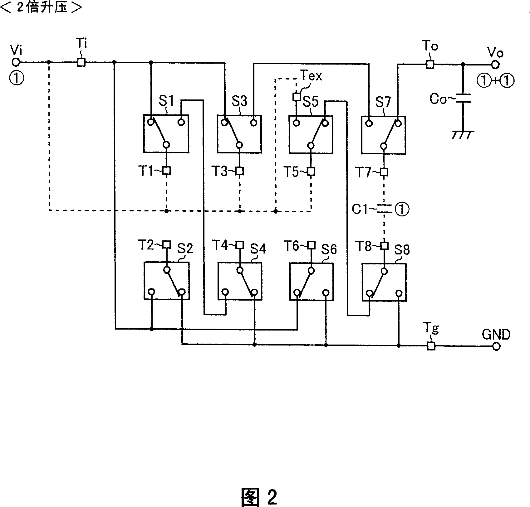
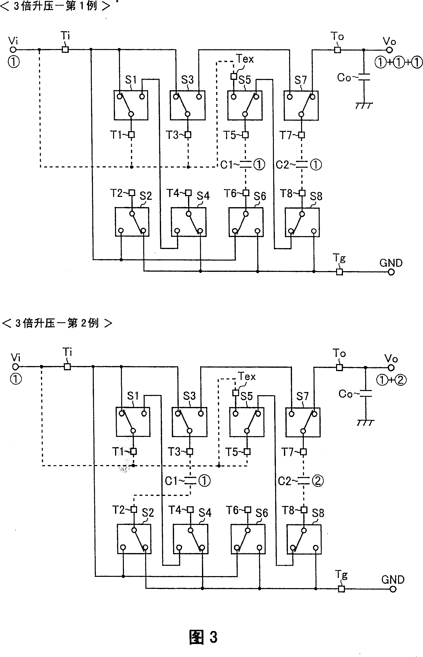
[0022] Hereinafter, the present invention will be described in detail by taking, as an example, a semiconductor integrated circuit device that can be used generally when constituting charge pump circuits of the 2-fold boost type to 7-fold boost type.

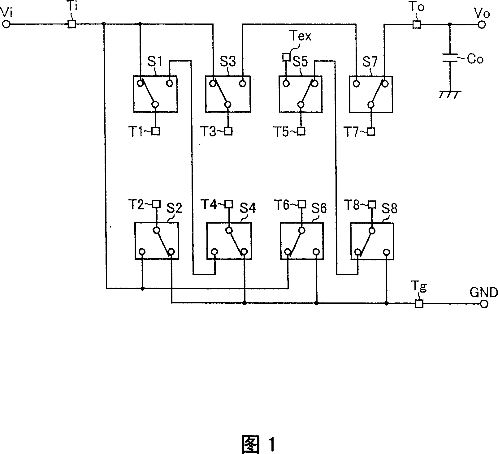
[0023] FIG. 1 is a diagram showing an embodiment of a semiconductor integrated circuit device of the present invention.

[0024] As shown in this figure, the semiconductor integrated circuit device of this embodiment has: an input terminal Ti to which an input voltage Vi is applied; an output terminal To for extracting an output voltage Vo; a ground terminal Tg to which a ground voltage GND is applied; The external terminals T1~T8 of capacitors for charge transfer (not shown in this figure) are externally connected; the switches S1~S8 for charge transfer composed of MOSFETs or bipolar transistors provided corresponding to the external terminals T1~T8, in addition, there are also optional The boost ratio switching terminal Tex th...


PUM


Abstract

In addition to an input terminal, an output terminal, a ground terminal, a plurality of external terminals, and a plurality of charge transfer switches, a semiconductor integrated circuit device has a step-up factor switching terminal. Here, the plurality of charge transfer switches each have a common contact connected to corresponding one of the plurality of external terminals and two selection contacts alternatively connected to the common contact, and one of the selection contacts of the plurality of charge transfer switches is connected to the step-up factor switching terminal, and each of the other selection contacts is connected to one of the input terminal, the output terminal, the ground terminal, and the rest of the other selection contacts. With this configuration, it is possible to make the semiconductor integrated circuit device versatile so that it can be used to form charge pump circuits having different step-up factors.

Description

technical field [0001] The invention relates to a semiconductor integrated circuit device used in a charge pump circuit, in particular to a variable boosting ratio technology. Background technique [0002] FIG. 9 is a circuit diagram showing a conventional example of a charge pump circuit. In addition, the charge pump circuit 100 in this figure is configured to periodically turn on / off a plurality of charge transfer switches 101 to 104 based on a clock signal (not shown), and charge and discharge the charge transfer capacitor 105, A desired output voltage Vo (=2Vi) is generated based on the input voltage Vi. [0003] The above-mentioned positive boosting operation will be specifically described. When generating the output voltage Vo, first, as a charging period, the switches 101 and 102 are turned on, and the switches 103 and 104 are turned off. Through this switching control, the input voltage Vi is applied to one end (point A) of the capacitor 105, and the ground voltag...

Claims


Application Information

Patent Timeline
Patent Type & Authority Applications(China)
IPC IPC(8): H02M3/07H01L27/04
CPCH02M3/07
Inventor 今中义德
Owner ROHM CO LTD
Why Eureka
Try Eureka