Multilayer printed wiring board and method of measuring characteristic impedance

A multi-layer printing and wiring board technology, applied in the direction of measuring resistance/reactance/impedance, measuring electricity, printed circuit, etc., can solve the problem of taking a long time to measure, increasing the sample area, and it is difficult to accurately measure the characteristic impedance and other problems, to achieve the effect of efficiently measuring characteristic impedance and reducing the occupied area

Active Publication Date: 2007-09-26
NEC CORP
View PDF1 Cites 15 Cited by
  • Summary
  • Abstract
  • Description
  • Claims
  • Application Information

AI Technical Summary

Problems solved by technology

However, in this technique, the characteristic impedance of the signal wiring on the printed board is calculated by measuring the cross-sectional shape of the wiring formed as a sample, so it is difficult to measure the characteristic impedance accurately
In order to measure the characteristic impedance electrically accurately, a sample having the shape shown in Fig. 6 is required, so the area occupied by the sample increases
[0006] In addition, when measuring the characteristic impedance using a conventional sample as shown in FIG. 6, it is necessary to measure the characteristic impedance of each signal wiring layer separately using the TDR (Time Domain Reflectometry) method, so it takes a long time to perform the measurement.

Method used


Image

  • Multilayer printed wiring board and method of measuring characteristic impedance
  • Multilayer printed wiring board and method of measuring characteristic impedance
  • Multilayer printed wiring board and method of measuring characteristic impedance

Examples


Embodiment Construction

[0022] Hereinafter, exemplary embodiments according to the present invention will be described with reference to the accompanying drawings.

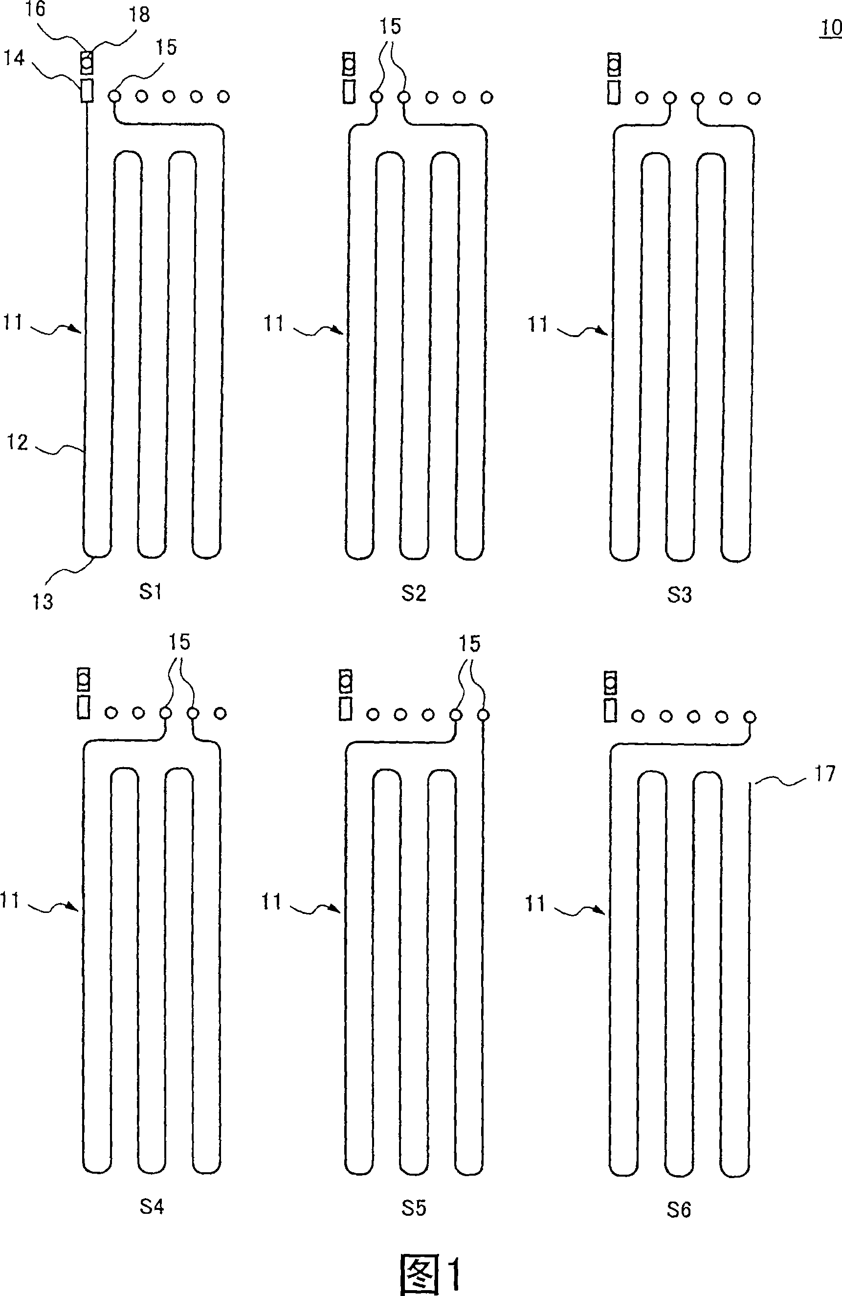
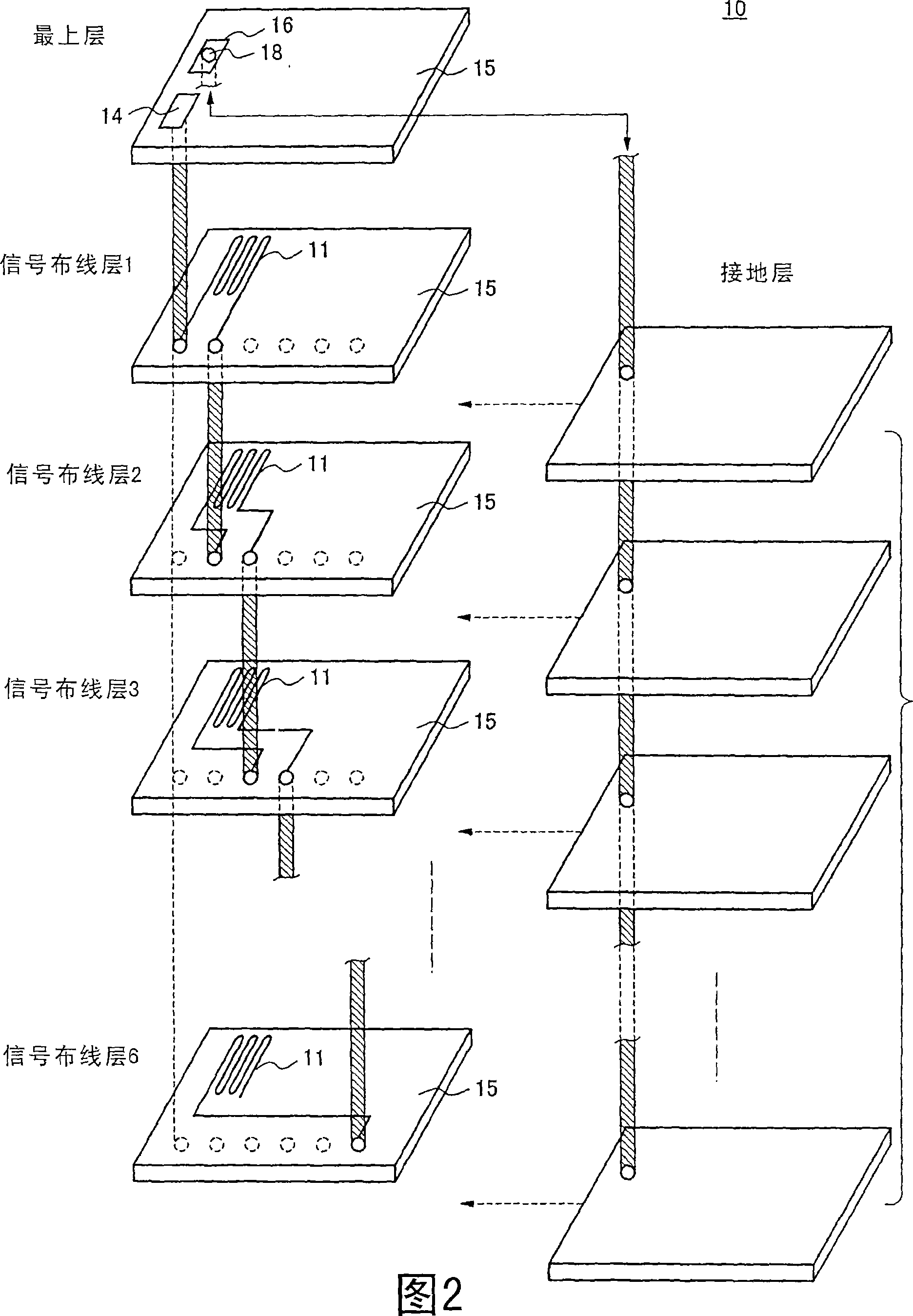
[0023] FIG. 1 is a plan view showing a wiring pattern of a sample formed on each signal wiring layer in a multilayer printed wiring board 10 according to an embodiment of the present invention. In addition, FIG. 2 is an exploded perspective view schematically showing the multilayer printed wiring board 10 according to the embodiment of the present invention.

[0024] Each sample formed on the multilayer printed wiring board 10 is composed of an individual sample (pattern wiring part) 11 formed on the wiring board of each signal wiring layer and a channel connecting the pattern wiring parts 11 of the respective signal wiring layers to each other. Hole 15 constitutes. The pattern wiring part 11 protrudes from the connecting portion with the through hole 15, and is composed of six linear portions 12 and a turn-back portion 13 having a widt...


PUM


Abstract

A multilayer printed wiring board having a compact test coupon formed on each of the signal wiring layers is provided, and accurate and efficient method of characteristic impedance measurement for each signal wiring layer is realized. The test coupon is constituted by a plurality of linear parts extending parallel to each other and folded-back parts mutually connecting the linear parts. A through hole is provided for serially connecting the respective test coupons of the signal wiring layers adjoining each other. Two measuring pads, one is connected to one end of the serially connected test coupons and another is connected to the ground layer, are also provided. The measurement is performed by applying a step pulse between two measuring pads and measuring voltages of reflection waves from the serially connected test coupons.

Description

technical field [0001] The present invention relates to a multilayer printed wiring board on which electronic circuit components are mounted, and a method of measuring characteristic impedance of signal wiring formed on the multilayer printed wiring board. More specifically, the present invention relates to a technique for measuring the characteristic impedance of signal wiring of a multilayer printed wiring board using a TDR (Time Domain Reflectometry) method. Background technique [0002] In recent years, as the density requirements for printed wiring boards have increased, a plurality of wiring boards formed with wiring patterns (patterns) on them have been pressed into three or more layers including the surface wiring board layer. A multilayer printed wiring board is formed. In addition, the operating speed of electronic circuit components mounted on multilayer printed wiring boards is also increasing. In an electronic circuit element operating at high speed, reflected...

Claims


Application Information

Patent Timeline
Patent Type & Authority Applications(China)
IPC IPC(8): H05K1/02H05K1/16G01R27/00
CPCG01R31/2818H05K1/0237H05K1/0268H05K3/429H05K3/4611H05K2201/09263G01R31/2813
Inventor 江藤顺
Owner NEC CORP
Why Eureka
Try Eureka