Measuring method and apparatus using attenuation in total reflection
- Summary
- Abstract
- Description
- Claims
- Application Information
AI Technical Summary
Benefits of technology
Problems solved by technology
Method used
Image
Examples
first embodiment
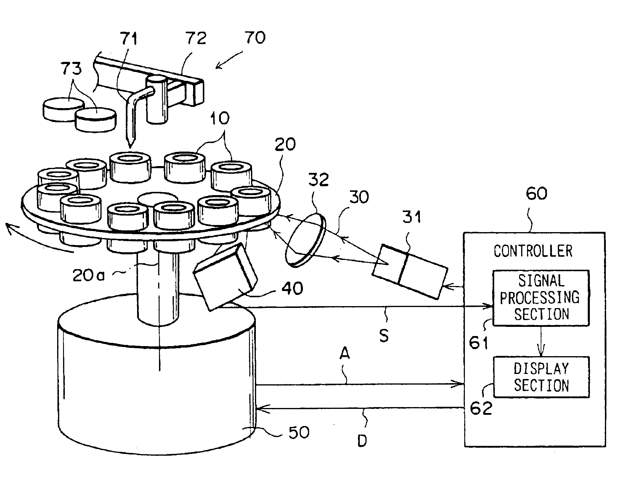
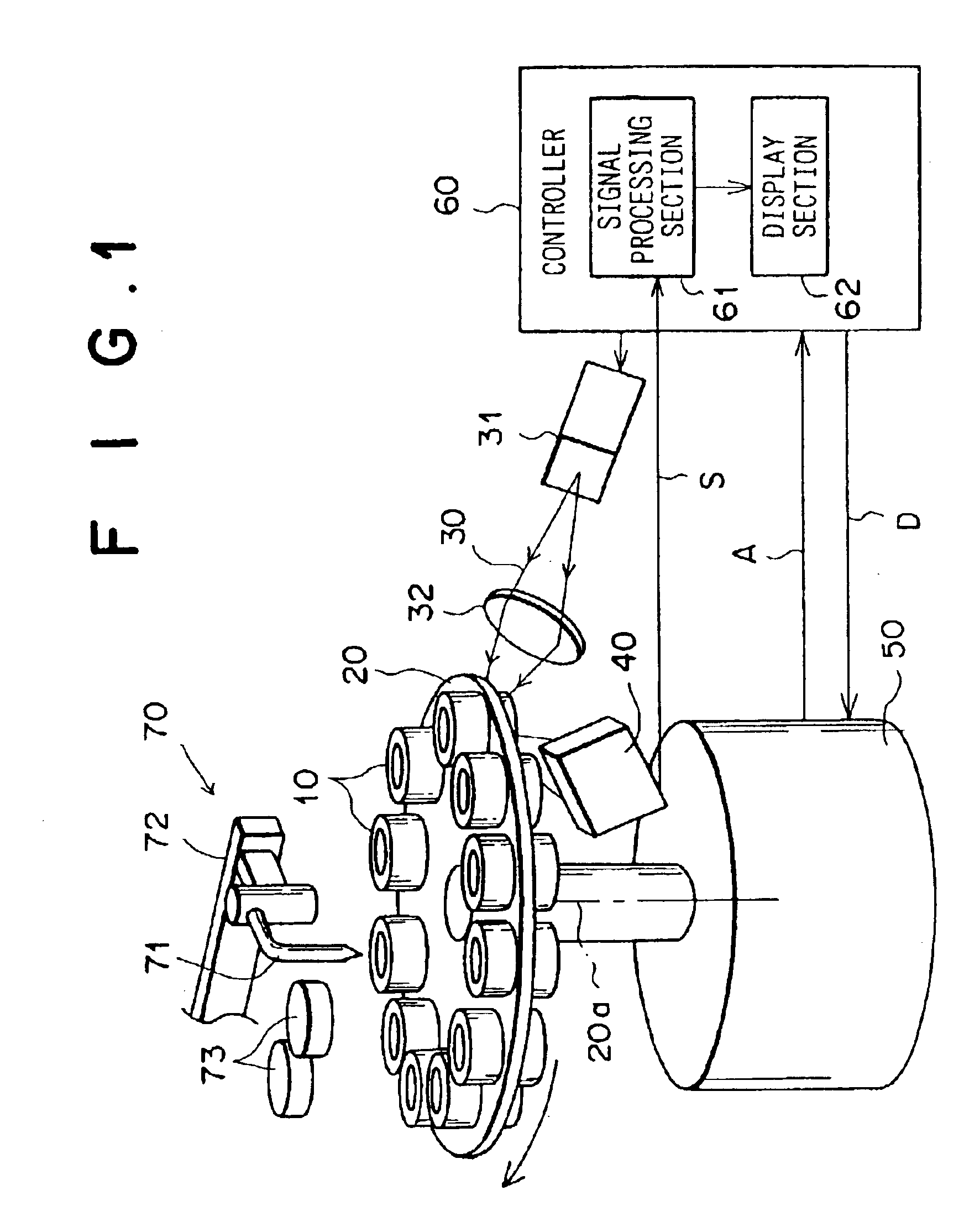
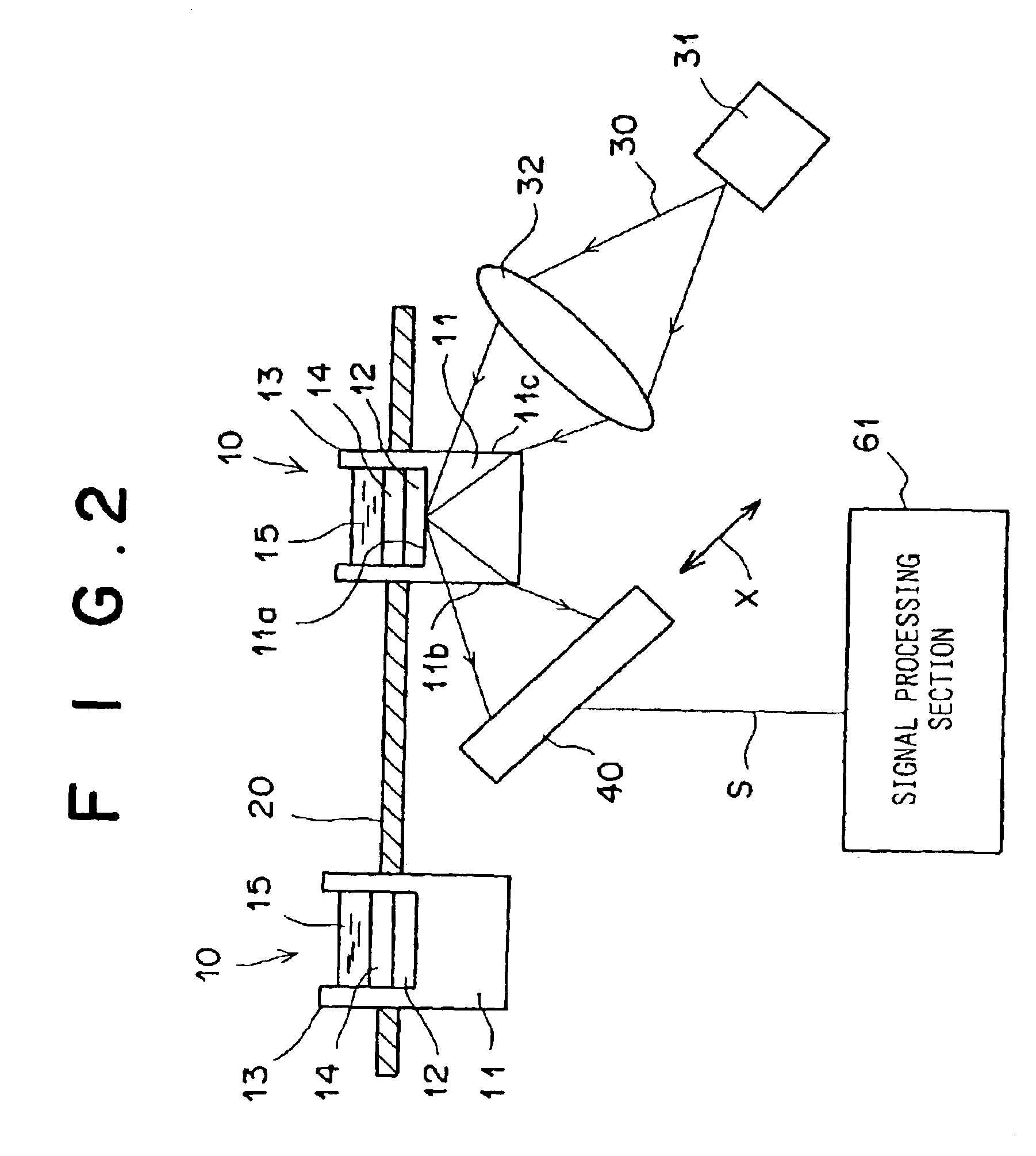
Embodiments of the present invention will be described in detail with reference to the drawings, hereinbelow. FIG. 1 shows the overall arrangement of a surface plasmon resonance sensor in accordance with the present invention, and FIG. 2 is a side view showing an important part of the surface plasmon resonance sensor.
As shown in FIG. 1, the surface plasmon resonance sensor comprises a turn table 20 on which a plurality of measuring units 10 are supported, a laser 31 such as a semiconductor laser which emits a measuring light beam (laser beam) 30, a condenser lens 32 which forms an incident optical system, a photodetector 40, a drive means 50 which intermittently rotates the turn table 20, a controller 60 which controls the drive means 50 and at the same time receives output signal S of the photodetector 40 to execute processing described later, and an automatic sample supply mechanism 70.
As shown in FIG. 2, each of the measuring units 10 comprises a transparent dielectric block 11 w...
fifth embodiment
A fifth embodiment of the present invention will be described, hereinbelow. FIG. 9 is a side view showing a measuring apparatus utilizing the phenomenon of attenuation in total internal reflection in accordance with the present invention. In FIG. 9, elements analogous to those shown in FIG. 2 are given the same reference numerals.
The measuring apparatus of this embodiment is a leaky mode sensor and measuring units 110 in the form of a measuring chip are employed in this embodiment. Each measuring unit 110 comprises a dielectric block 11, a clad layer 111 formed on one surface (the upper surface as seen in FIG. 9) and an optical waveguide layer 112 formed on the clad layer 111.
The dielectric block 11 is formed of, for instance, synthetic resin or optical glass such as BK7. The clad layer 111 is formed of dielectric material lower than the dielectric block 1 in refractive index or metal such as gold. The optical wave guide layer 112 is formed of dielectric material such as PMMA which ...
sixth embodiment
A sixth embodiment of the present invention will be described, hereinbelow. FIG. 10 is a side view showing an important part of a measuring apparatus utilizing the phenomenon of attenuation in total internal reflection in accordance with the present invention. In FIG. 10, elements analogous to those shown in FIG. 9 are given the same reference numerals.
The measuring apparatus of this embodiment is also a leaky mode sensor and measuring units 120 in the form of a measuring chip are employed in this embodiment. Each measuring unit 120 comprises a dielectric block 11, a clad layer 111 formed on one surface (the upper surface as seen in FIG. 9) of the dielectric block 11, an optical waveguide layer 112 formed on the clad layer 111 and a sensing medium 14 fixed on the optical waveguide layer 112. The apparatus of this embodiment basically differs from that shown in FIG. 9 only in that the sensing material 14 is fixed on the optical waveguide layer 112.
The sensing medium 14 fixed on the s...
PUM
 Abstract
Description
Claims
Application Information


