

Method for producing liquid crystal display
A technology of liquid crystal display and manufacturing method, which is applied in the direction of manufacturing tools, instruments, transistors, etc., and can solve the problems of not meeting economic benefits, inefficient liquid crystal display technology, and lengthy test time for attaching time test cards, etc.
- Summary
- Abstract
- Description
- Claims
- Application Information
AI Technical Summary
Problems solved by technology
Method used
Image

Examples
Embodiment 1
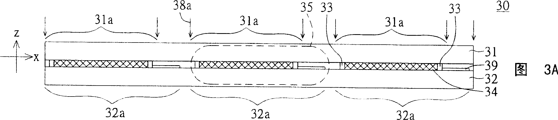
[0042] Please refer to Figures 2-3F at the same time. Figure 2 shows a flowchart of a method for manufacturing a liquid crystal display according to Embodiment 1 of the present invention, and Figures 3A-3F show a liquid crystal display according to Embodiment 1 of the present invention. sectional view of the process. First, in step 21, a panel-to-group structure 30 is provided, as shown in FIG. 3A. In Figure 3A, the panel pair structure 30 includes a first substrate 31 and a second substrate 32 arranged parallel to each other and several frame glues 33, and the frame glue 33 connects the inside of the first substrate 31 and the second substrate 32 surface. The first substrate 31 includes several third substrates 31a, the second substrate 32 includes several fourth substrates 32a corresponding to these third substrates 31a, each third substrate 31a, each fourth substrate 32a and each frame glue 33 are form a panel. If the panel contains liquid crystals, the panel is a liquid...
Embodiment 2
[0060]Please refer to Figures 8-9G at the same time. Figure 8 shows a flowchart of a method for manufacturing a liquid crystal display according to Embodiment 2 of the present invention, and Figures 9A-9G show a liquid crystal display according to Embodiment 2 of the present invention. sectional view of the process. First, in step 81, a panel-to-group structure 30 is provided, as shown in FIG. 9A. In Figure 9A, the panel pair group structure 30 includes a first substrate 31 and a second substrate 32 arranged parallel to each other and several frame glues 33, and the frame glue 33 connects the inside of the first substrate 31 and the second substrate 32 surface. The first substrate 31 includes several third substrates 31a, the second substrate 32 includes several fourth substrates 32a corresponding to these third substrates 31a, each third substrate 31a, each fourth substrate 32a and each frame glue 33 are form a panel. If the panel contains liquid crystals, the panel is a l...
Embodiment 3
[0070] Please refer to Figures 10-11H at the same time. Figure 10 shows a flowchart of a method for manufacturing a liquid crystal display according to Embodiment 3 of the present invention, and Figures 11A-11G show a liquid crystal display according to Embodiment 3 of the present invention. sectional view of the process. First, in step 81, a panel-to-group structure 30 is provided, as shown in FIG. 11A. In Figure 11A, the panel pair group structure 30 includes a first substrate 31 and a second substrate 32 arranged parallel to each other and several frame glues 33, and the frame glue 33 connects the inside of the first substrate 31 and the second substrate 32 surface. The first substrate 31 includes several third substrates 31a, the second substrate 32 includes several fourth substrates 32a corresponding to these third substrates 31a, each third substrate 31a, each fourth substrate 32a and each frame glue 33 are form a panel. If the panel contains liquid crystals, the pane...
PUM
 Abstract
Description
Claims
Application Information