Substrate check device and substrate check method

A substrate inspection and substrate technology, applied in the direction of image detector method and image signal processing, measuring device, optical device, etc., can solve the problems of difficult measurement, and achieve the effect of correctly measuring pattern defects

Inactive Publication Date: 2007-10-10
SAMSUNG DISPLAY CO LTD
View PDF0 Cites 30 Cited by
  • Summary
  • Abstract
  • Description
  • Claims
  • Application Information

AI Technical Summary

Problems solved by technology

[0005] However, in the conventional substrate inspection, the operator judges whether there is a defect with the naked eye while irradiating light on the patterned substrate, so there is a problem that it is difficult to perform accurate measurement

Method used


Image

  • Substrate check device and substrate check method
  • Substrate check device and substrate check method
  • Substrate check device and substrate check method

Examples


Embodiment Construction

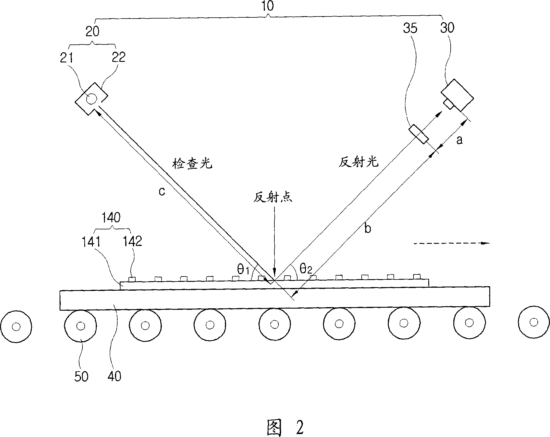
[0067] Hereinafter, the present invention will be described with reference to the accompanying drawings.

[0068] In various embodiments, the same reference numerals are attached to the same components, and the same components are typically described in the first embodiment, and may be omitted in other embodiments.

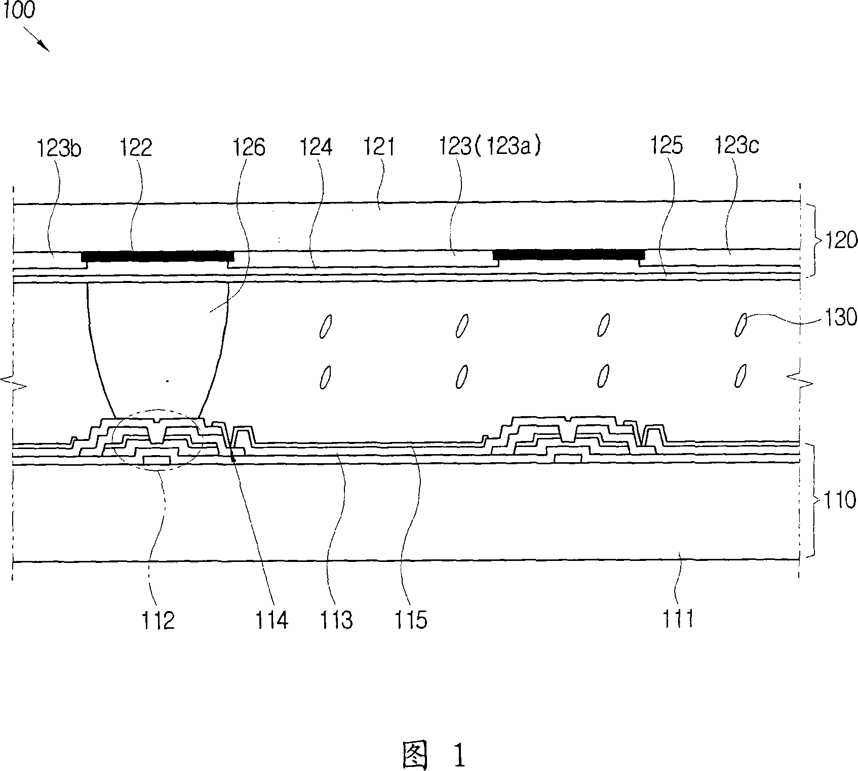
[0069] In the following embodiments, a color filter substrate of a liquid crystal display device will be described as an example of a substrate, but the present invention can also be applied to a thin film transistor substrate. In addition, the present invention can also be applied to substrates of other display devices such as organic electroluminescent devices (OLEDs), electrophoretic display devices (EPD), and plasma display devices (PDP).

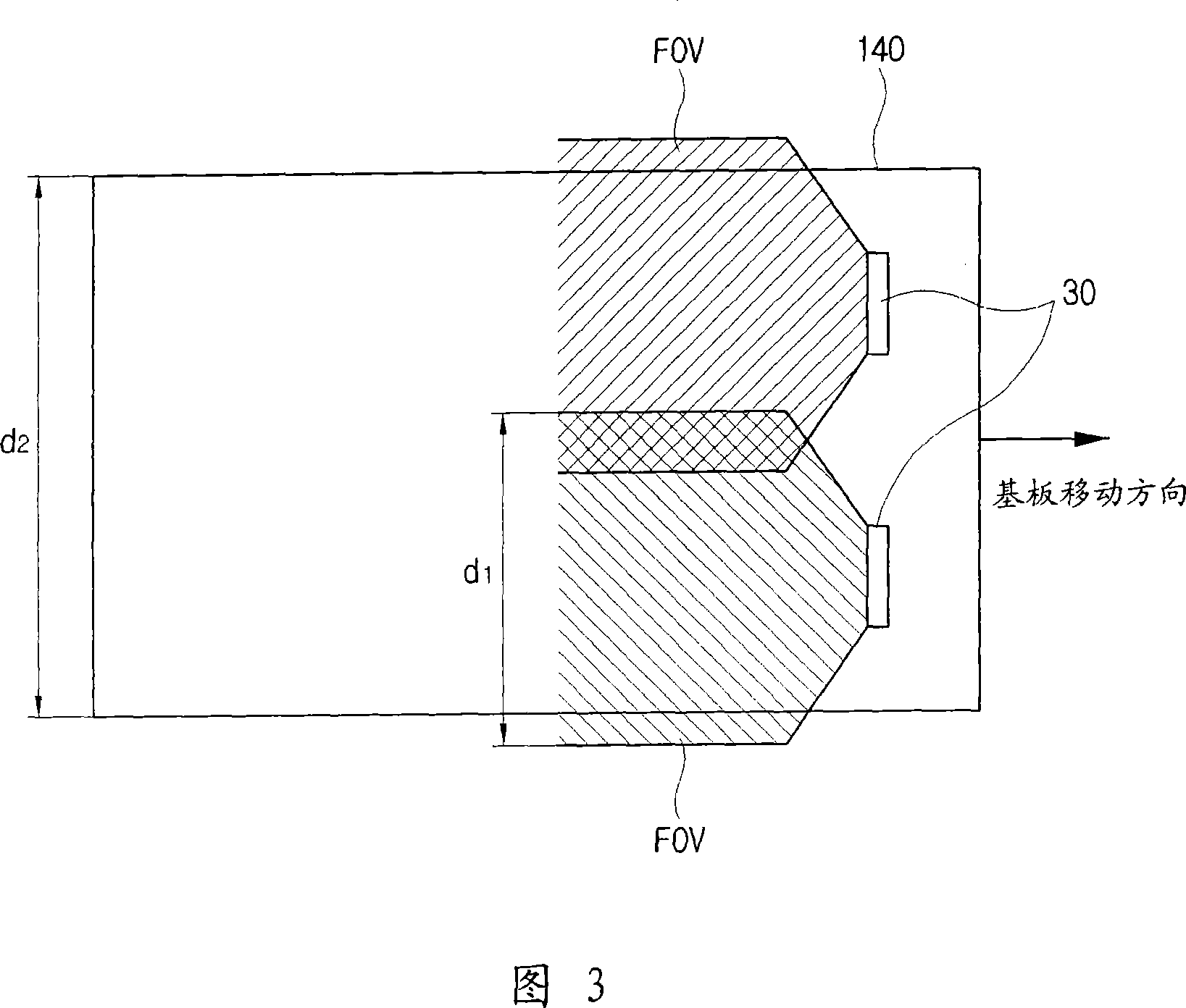
[0070] In the following description, the size of a pixel region refers to the length of one side of a square having the same area as the area of ​​the pixel region. Each imaging unit has a square shape, and the size of the...


PUM


Abstract

The present invention provides a method and apparatus for inspecting substrate which can correctly measuring and determining the defect of the pattern, the method for inspecting substrate comprises steps of: applying inspecting light on the substrate forming pattern, inspecting the brightness of the inspecting light reflected by the substrate, and estimating whether the pattern has defect according to inspected brightness.

Description

technical field [0001] The present invention relates to a substrate inspection device and a substrate inspection method using the same, and more specifically, to a substrate inspection device capable of accurately measuring pattern defects on a substrate and a substrate inspection method using the same. Background technique [0002] Recently, instead of existing Braun tubes, flat panel display devices such as liquid crystal display devices and organic electroluminescent devices (OLEDs) are widely used. [0003] Substrates formed with various patterns are used in these display devices. For example, patterns such as a black matrix and color filters are formed on a color filter substrate of a liquid crystal display device. Such a pattern must be formed to a uniform height. In the case of a color filter, if the formed height is not uniform, a mottling pattern may be generated on the screen. [0004] During the manufacturing process of the display device, it is checked whether...

Claims


Application Information

Patent Timeline
Patent Type & Authority Applications(China)
IPC IPC(8): H01L21/66G01N21/88G01N21/892G01B11/00G01B11/30G01R31/308G02F1/133G02B5/20
CPCG01N21/8806G01N21/89G01N2021/177G02F1/1309
Inventor 孙亨一金永日梁廷郁全灿济
Owner SAMSUNG DISPLAY CO LTD
Why Eureka
Try Eureka