Multiplexing a parallel bus interface and a flash memory interface
A technology of flash memory and bus interface, which is applied in the system field of multiplexing parallel bus interface and flash memory interface, and can solve the problems of high cost and undesired incremental cost
- Summary
- Abstract
- Description
- Claims
- Application Information
AI Technical Summary
Problems solved by technology
Method used
Image

Examples
Embodiment Construction
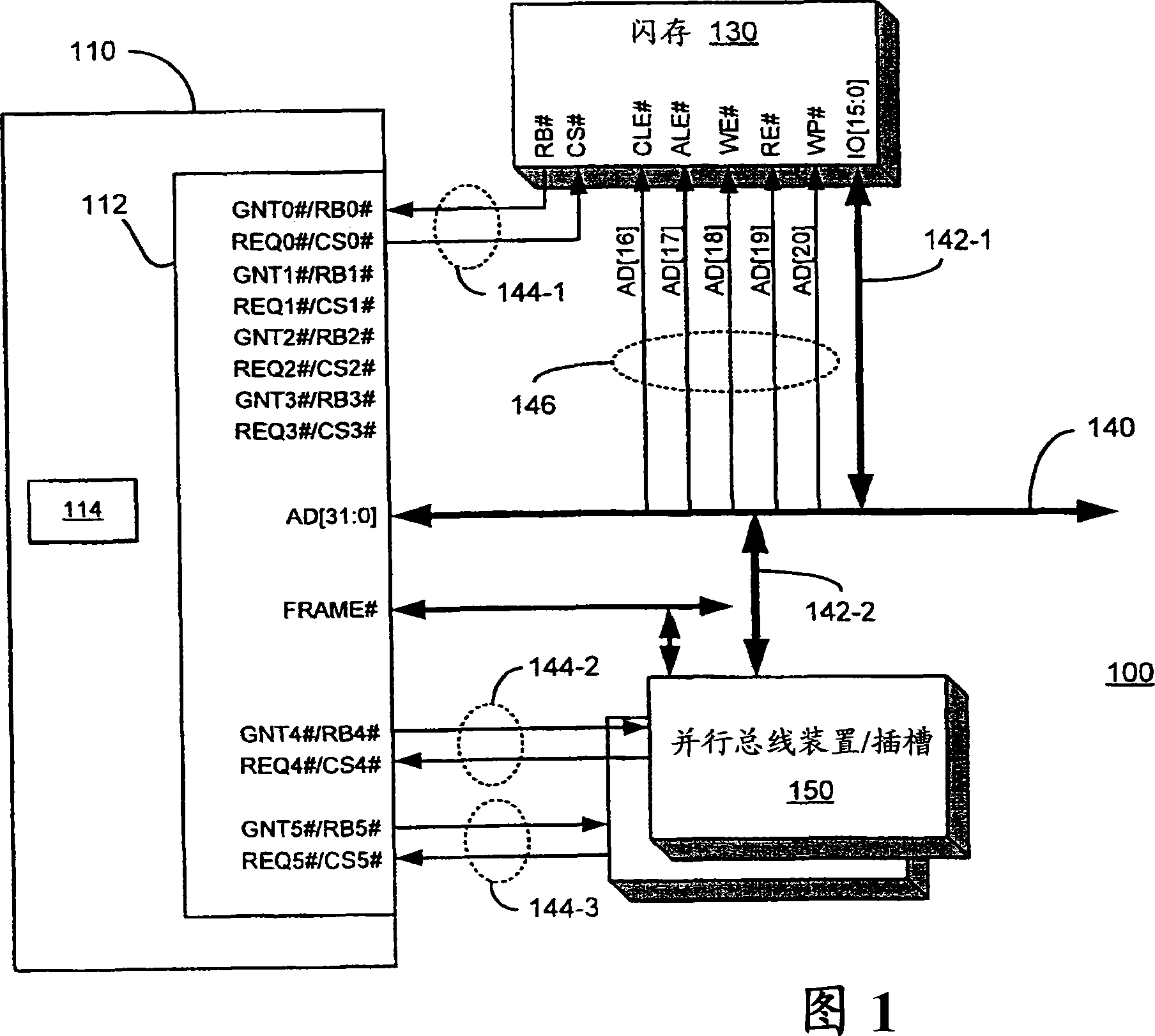
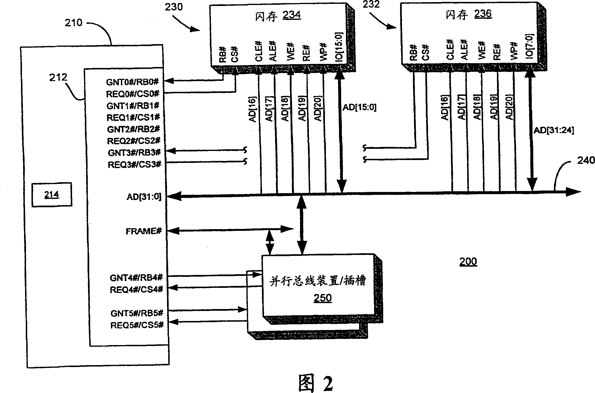
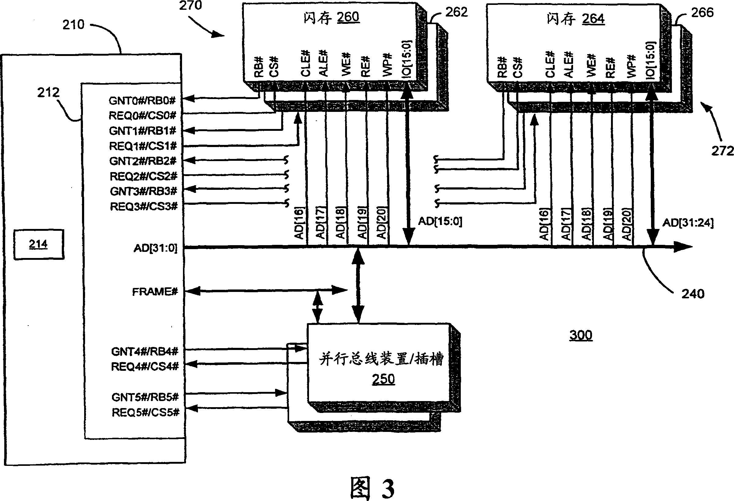
[0032] Embodiments of the present invention allow chipsets to integrate a flash memory interface (with virtually no added pin cost) by multiplexing selected interface signals over an existing parallel bus interface. In some embodiments, the flash memory interface signals are multiplexed over an existing peripheral component interconnect (PCI) interface. In such embodiments, one or more PCI devices and one or more NAND flash devices may be connected to the same bus. The chipset can dynamically select whether the PCI device or the NAND flash device has access to the bus. In an alternative embodiment, the selection can be made statically, such that either PCI devices or NAND flash devices can be used, but one system cannot use both.
[0033] FIG. 1 is a block diagram illustrating selected aspects of a computing system capable of multiplexing flash memory interface signals over a parallel bus interface, according to one embodiment of the invention. System 100 includes integrated...
PUM
 Abstract
Description
Claims
Application Information