A double-fin channel wrap gate field-effect transistor and its manufacture method

A field effect transistor, double fin technology, applied in the field of metal oxide semiconductor field effect transistors, can solve the problems of reduced device switching speed, limited effective channel width, increased gate capacitance, etc., so as to improve device switching speed, device Switching speed advantage, effect of reducing parasitic gate capacitance

Inactive Publication Date: 2007-10-24
PEKING UNIV
View PDF0 Cites 20 Cited by
  • Summary
  • Abstract
  • Description
  • Claims
  • Application Information

AI Technical Summary

Problems solved by technology

[0003] However, the reported nanowire devices and nanoscale gate-enclosed devices are either limited by the structure itself, or will bring difficulties in process preparation, etc., so that the advantages of nanowire devices and gate-enclosed devices are often not fully reflected.
[0004] For example, the nanowire Ω gate shown in Document 1 (F.L.Yang, D.H.Lee, H.Y.Chen, et al., "5nm-gate nanowire FinFET", in Symp.VLSI Tech.Dig., 2004, pp:196-197) Devices (as shown in Figure 1(a)-(d)) have the following problems: (1) they are prepared on SOI substrates, and the cost is very high; (2) since the preparation of silicon nanowires requires a very thin top silicon film, The channel on the SOI substrate has the same thickness as the silicon film of the source and drain, as shown in Figure 1(c), which increases the parasitic series resistance of the source and drain and limits the on-state drive current; (3) at the same time, the silicon nanowire The cross-sectional structure of the device along the vertical direction of the channel is an Ω gate structure, as shown in Figure 1(b) and (d), it is not a surrounding gate structure, and the gate control capability needs to be further improved
[0006] However, this double nanowire ga

Method used


Image

  • A double-fin channel wrap gate field-effect transistor and its manufacture method
  • A double-fin channel wrap gate field-effect transistor and its manufacture method
  • A double-fin channel wrap gate field-effect transistor and its manufacture method

Examples


Embodiment Construction

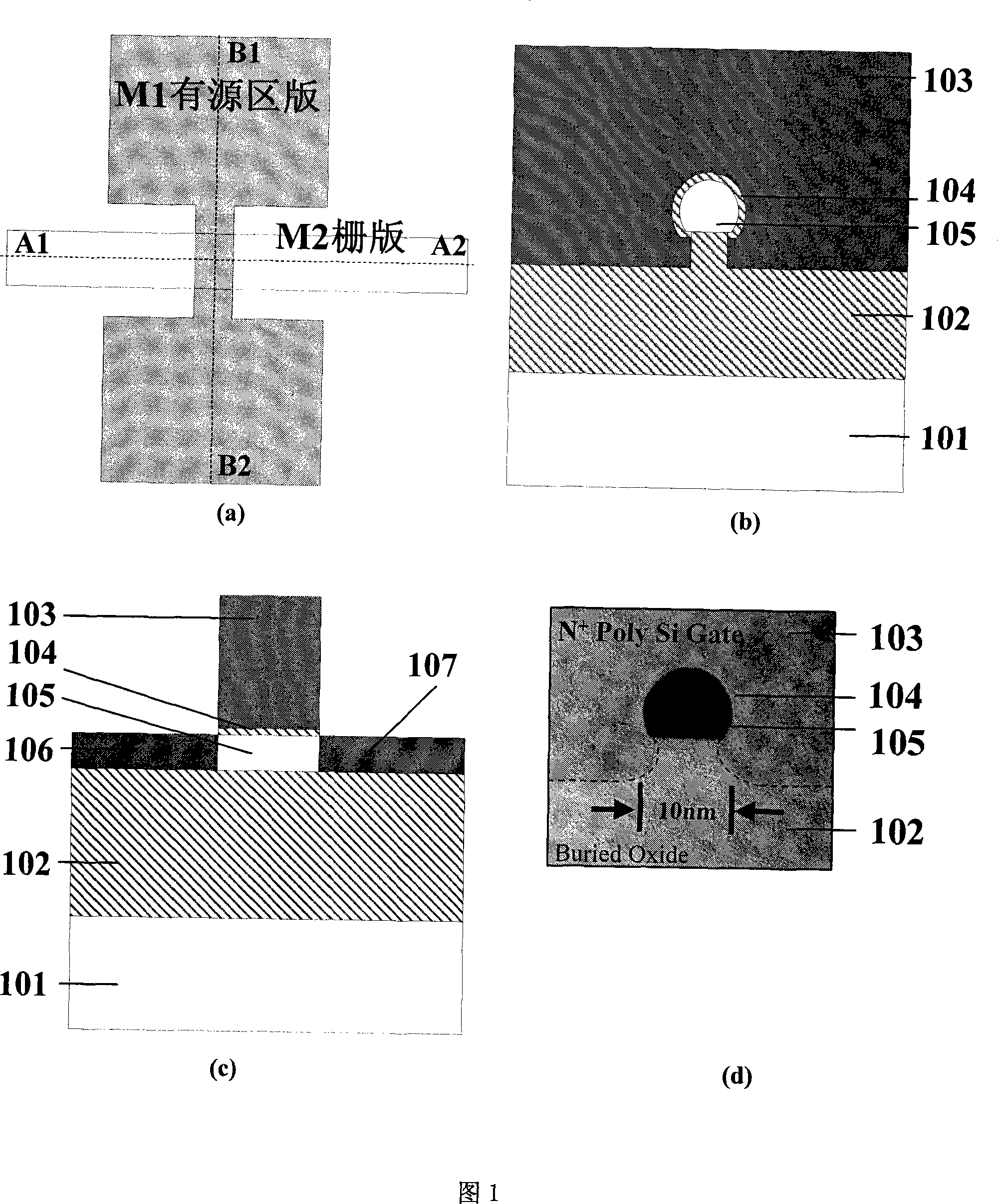
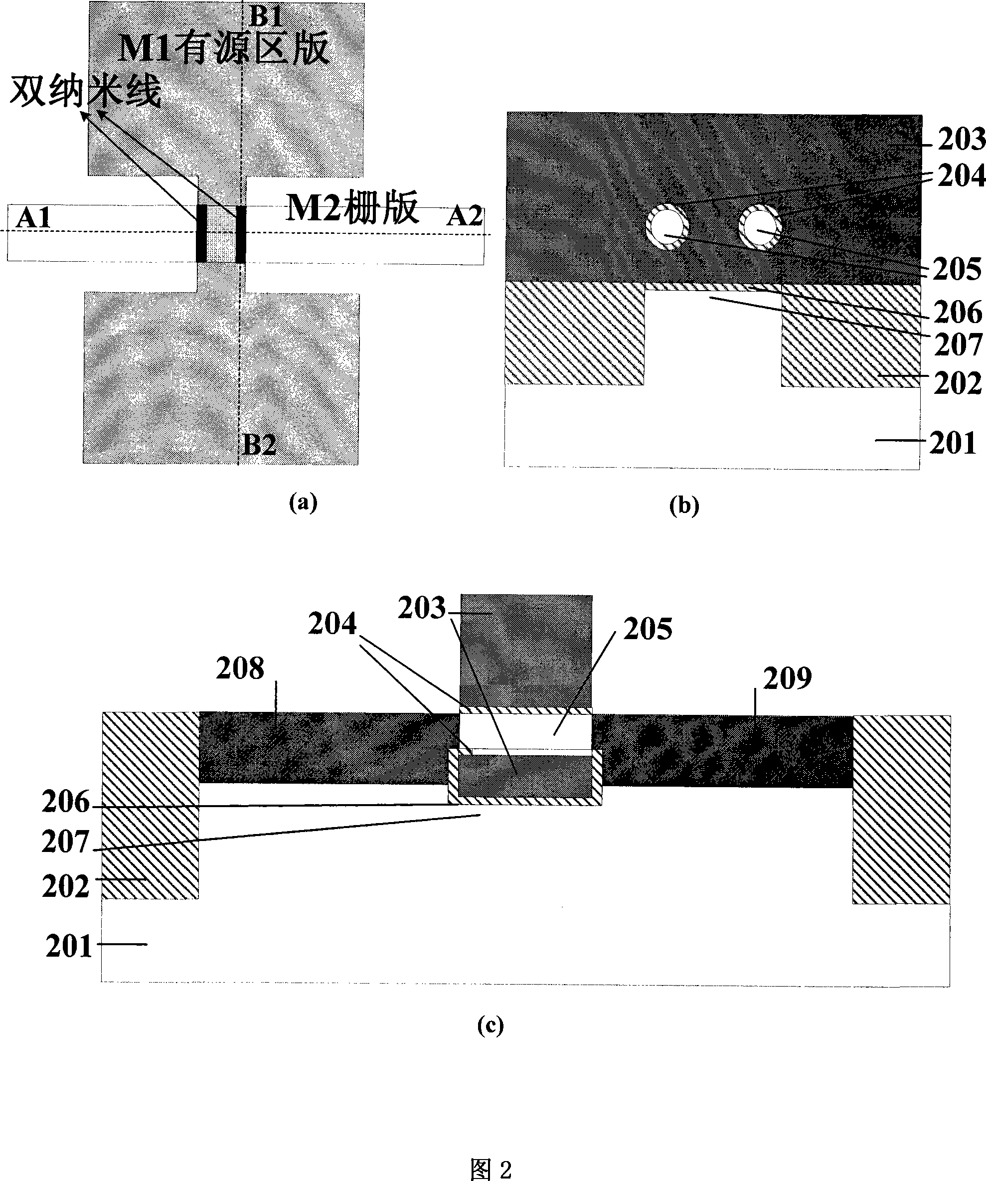
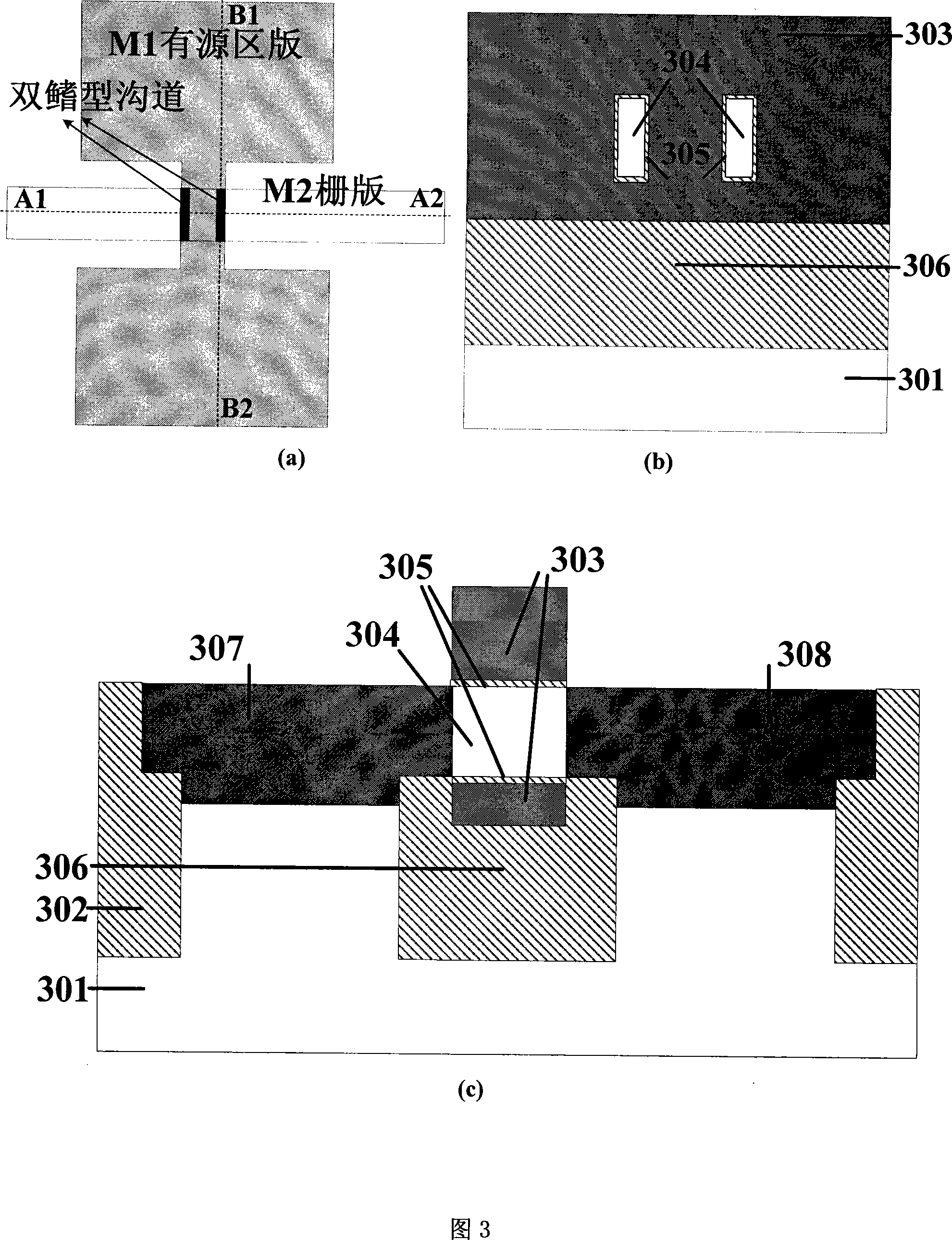
[0060] The double-fin trench-around-gate field effect transistor provided by the present invention and its manufacturing method will be described in detail below in conjunction with the accompanying drawings, but this does not constitute a limitation to the present invention.

[0061] As shown in FIG. 3 , it is a double-fin channel-around-gate device of this embodiment. The device is based on a bulk silicon substrate. From the cross-sectional structure along the vertical direction of the channel, the channel is two identical rectangular fins (Twin Fin), that is, a double-fin channel with a width ≤ 10nm and a height of 30-50nm. The channel width can reach 160-240nm; the double-fin channel is surrounded by gate oxide (Gate Oxide), and then by the gate (Gate), forming a gate-enclosed device; directly below the double-fin channel and between the substrate , there is a silicon dioxide insulating layer with a thickness of 150-250nm, forming a structure (Body-on-Insulator, BOI struc...


PUM

PropertyMeasurementUnit
Width waaaaaaaaaa
Heightaaaaaaaaaa
Thicknessaaaaaaaaaa

Abstract

The provided double-fin channel enclose-grid FET belonged to MOSFET technique in ULSI comprises: a silicon substrate, a grid anode and multicrystal silicon grid enclosing the channel to form the enclose-grid structure, both source and drain connecting with the substrate, two rectangular-section fins as the channels, and a thick SiO2 layer between the right bottom of channel and substrate. This invention reduces cost and power consumption, provides high-speed and high-performance circuit application.

Description

technical field [0001] The invention belongs to the technical field of metal oxide semiconductor field effect transistor (MetalOxide Silicon Field Effect Transistor-MOSFET) in ultra-large-scale integrated circuit (ULSI), and in particular relates to a double-fin type channel surrounding gate MOSFET and a preparation method thereof. Background technique [0002] With the wide application and high-speed development of integrated circuits, MOSFET technology has entered the nanometer field. When the gate length of conventional single-gate MOSFETs is scaled down to sub-50nm, problems such as poor gate control capability, deterioration of short channel effect, large leakage current and insufficient on-state drive current will become more and more serious. In order to improve the gate control capability of MOSFET (also called device), reduce leakage current, increase on-state drive current, increase switching ratio, and suppress short-channel effect, many double-gate or multi-gate ...

Claims


Application Information

Patent Timeline
IPC IPC(8): H01L29/78H01L21/336
Inventor 周发龙吴大可黄如王鹏飞诸葛菁张兴
Owner PEKING UNIV
Why Eureka
Try Eureka