Wide-band planar printed space fed antenna
A wide-band, planar technology, applied in the field of wide-band planar printed air-fed antennas, can solve the problems of antenna practical frequency band narrowing, inconvenient installation, low gain, etc., and achieve the effects of low cost, simple structure, and improved gain and aperture efficiency
- Summary
- Abstract
- Description
- Claims
- Application Information
AI Technical Summary
Problems solved by technology
Method used
Image

Examples
no. 1 example
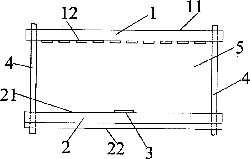
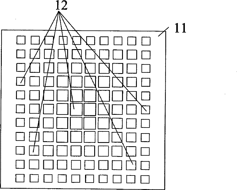
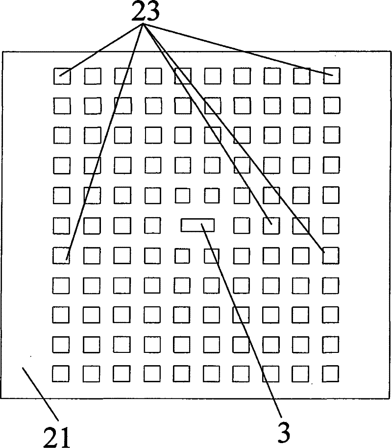
[0015] figure 1 It is a schematic diagram of the overall structure of the present invention, figure 2 It is a structural schematic diagram of the upper reflective cover plate of the embodiment of the present invention. Such as figure 1 , figure 2 The wide-band planar printed air-fed antenna of the present embodiment shown is composed of an upper reflector cover 1, a lower reflector base 2 and a feed source 3, and the upper reflector cover 1 is printed under it by an upper dielectric substrate 11 and 110 The surface is composed of mutually isolated upper metal patches 12, and the lower reflective base plate 2 is composed of a lower dielectric substrate 21 and a lower metal reflective plate 22 printed on its lower surface. The upper reflective cover plate 1 and the lower reflective base plate 2 are parallel to each other. The dielectric columns 4 are fixedly connected, and an air gap 5 with a thickness of 10.0 mm is provided between them. The feed source 3 is printed on the...
no. 2 example
[0018] see figure 1 . The wide-band planar printing air-feed antenna of this embodiment is made up of an upper reflection cover plate 1, a lower reflection base plate 2 and a feed source 3, and the upper reflection cover plate 1 is composed of an upper dielectric substrate 11 and 110 interconnections printed on its lower surface The isolated upper metal patch 12 is composed of the lower reflective base plate 2 composed of the lower dielectric substrate 21 and the lower metal reflective plate 22 printed on its lower surface. They are fixedly connected, and an air gap 5 with a thickness of 8.8mm is provided between the two, and the feed source 3 is printed on the upper surface of the lower dielectric substrate 21 . The upper dielectric substrate 11 is rectangular, its length, width and thickness are 70 mm, 63 mm and 1.6 mm in sequence, and its relative dielectric constant is 3.2. The shape, geometric dimension and relative permittivity of the lower dielectric substrate 32 are ...
PUM
 Abstract
Description
Claims
Application Information