

Article including sheet-like electromagnetic shielding structure
An electromagnetic shielding and structural technology, applied in the direction of magnetic/electric field shielding, shielding, shielding materials, etc., can solve problems such as high cost and affecting characteristics
- Summary
- Abstract
- Description
- Claims
- Application Information
AI Technical Summary
Problems solved by technology
Method used
Image

Examples
Embodiment 1
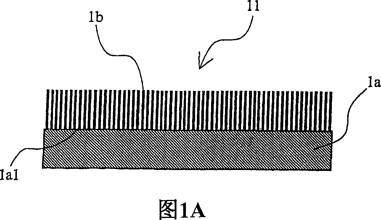
[0399] A hand-held phone including a sheet-like electromagnetic shielding structure was prepared by pressure-sensitively bonding the sheet-like electromagnetic shielding structure A1 prepared in Production Example 1 of the sheet-like electromagnetic shielding structure on the inner surface of the hand-held phone casing, using its surface fully exposed The electromagnetically conductive or absorbing pressure-sensitive adhesive layer (ie, the electromagnetically conductive or absorbing pressure-sensitive adhesive layer on which the electromagnetically conductive or absorbing fiber fine pile is not formed).
Embodiment 2
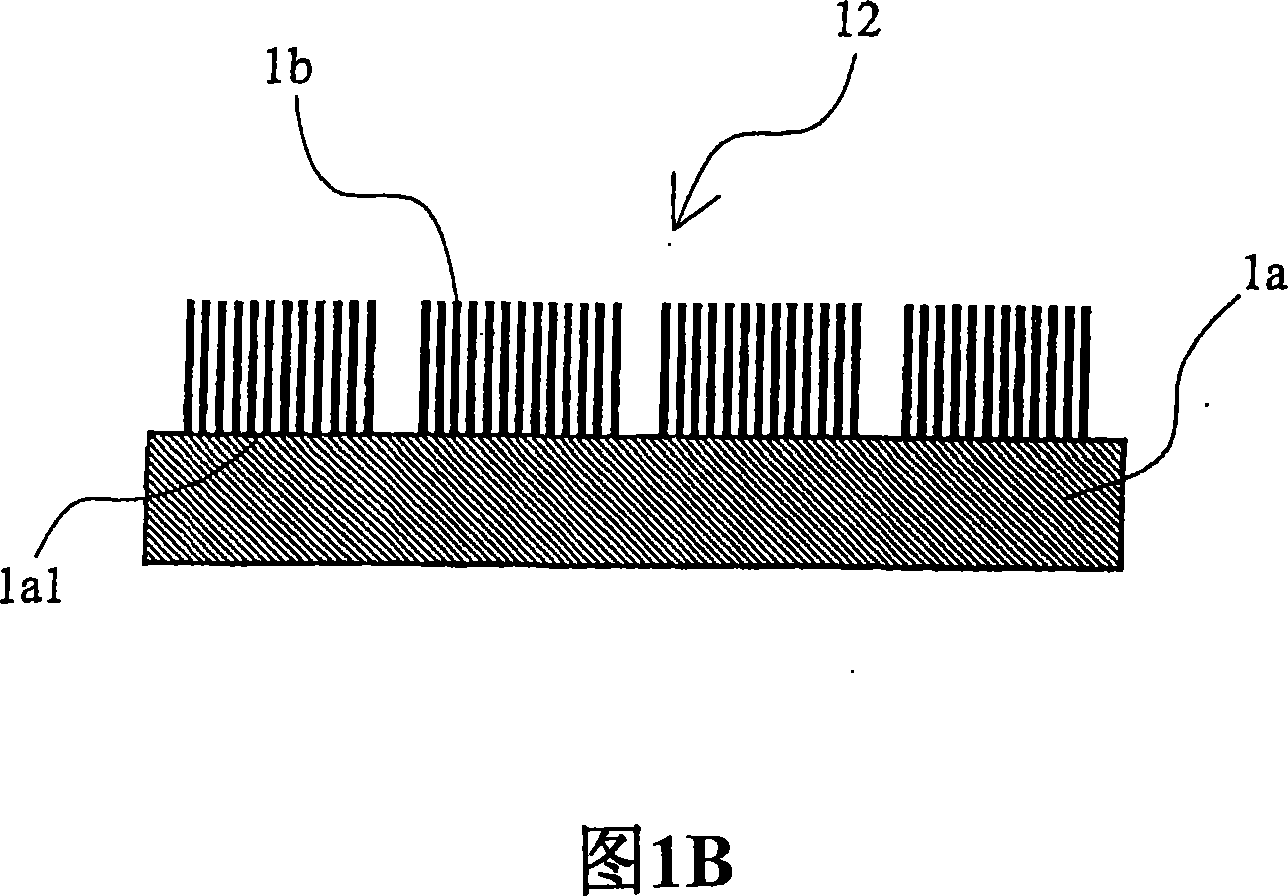
[0401] A handy phone including a sheet-like electromagnetic shielding structure was prepared by pressure-sensitively bonding the sheet-like electromagnetic shielding structure A2 prepared in Production Example 2 of the sheet-like electromagnetic shielding structure to the back of the liquid crystal display module unit inside the handy phone, using its An electromagnetically conductive or absorbing pressure sensitive adhesive layer with a fully exposed surface (ie, a layer of electromagnetically conducting or absorbing pressure sensitive adhesive on which no electromagnetically conductive or absorbing fiber fluff is formed).
Embodiment 3
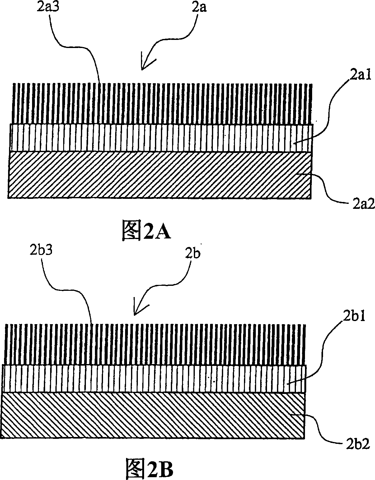
[0403] A handy phone including a sheet-like electromagnetic shielding structure was prepared by pressure-sensitively bonding the sheet-like electromagnetic shielding structure A3 prepared in Production Example 3 of the sheet-like electromagnetic shielding structure to the back of the circuit board inside the handy phone, using non-electromagnetic conduction or absorbent pressure sensitive adhesive layer.
PUM
 Abstract
Description
Claims
Application Information