Semiconductor device and its manufacturing method
A manufacturing method, semiconductor technology, applied in the direction of semiconductor/solid-state device manufacturing, semiconductor devices, semiconductor/solid-state device components, etc., can solve the problems of conductor thinning and disappearing, and cannot fully suppress interference in high-concentration areas, so as to prevent thinning and disappearance, reducing junction leakage current, and preventing the reduction of active region width
- Summary
- Abstract
- Description
- Claims
- Application Information
AI Technical Summary
Problems solved by technology
Method used
Image

Examples
Embodiment approach 1
[0130] figure 1 is a cross-sectional view showing a schematic structure of the semiconductor device according to Embodiment 1 of the present invention. This semiconductor device has thin trench isolations 30 and 30 ′ in which a polysilicon film 4 as a conductive film is disposed through a silicon oxide film 3 in a trench 2 provided in a silicon substrate 1 as a semiconductor substrate. Here, in the trench-type element isolation 30 , the polysilicon film 4 arranged in the trench 2 is arranged on the entire surface over the entire trench width on the bottom surface in the trench 2 . In addition, in the trench-type element isolation 30 ′, the polysilicon film 4 arranged in the trench 2 is arranged only on the sidewall side of the bottom surface in the trench 2 , and is not arranged on substantially the bottom surface of the trench 2 . Near the central part.
[0131] In trench-type element isolation 30 , the height of polysilicon film 4 is lower than the surface of silicon subs...
Embodiment approach 2
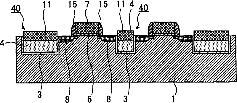
[0157] Figure 13 It is a cross-sectional view showing a schematic structure of a semiconductor device according to Embodiment 2 of the present invention. In this semiconductor device, there is a thin trench-type element isolation 40 in which a polysilicon film 4 as a conductive film is disposed through a silicon oxide film 3 in a trench 2 provided in a silicon substrate 1 as a semiconductor substrate. Here, in the trench-type element isolation 40 , the polysilicon film 4 is arranged on the entire surface over the entire trench width on the bottom surface in the trench 2 .
[0158] In trench-type element isolation 40 , the height of polysilicon film 4 is lower than the surface of silicon substrate 1 . Furthermore, the height of polysilicon film 4 in trench-type element isolation 40 is almost constant throughout trench-type element isolation 40 independent of the width of trench-type element isolation, that is, the trench width of trench 2 . However, the height of the remaini...
Embodiment approach 3
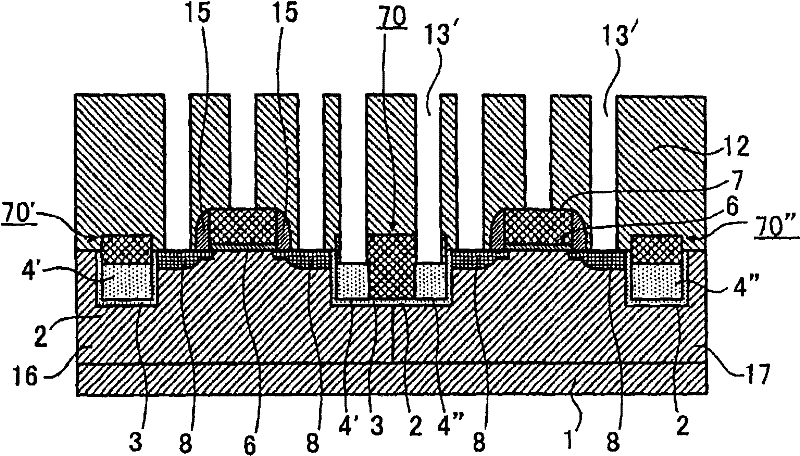
[0183] Figure 25 It is a cross-sectional view showing a schematic structure of a semiconductor device according to Embodiment 3 of the present invention. This semiconductor device has a thin trench isolation 40 in which a polysilicon film 4 as a conductive film is disposed through a silicon oxide film 3 in a trench 2 provided in a silicon substrate 1 as a semiconductor substrate. Here, in the trench-type element isolation 40 , the polysilicon film 4 is arranged on the entire surface over the entire trench width on the bottom surface in the trench 2 .
[0184] In trench-type element isolation 40 , the height of polysilicon film 4 is lower than the surface of silicon substrate 1 . Furthermore, the height of polysilicon film 4 in trench-type element isolation 40 is almost constant throughout trench-type element isolation 40 independent of the width of trench-type element isolation, that is, the trench width of trench 2 . However, the height of the remaining polysilicon film 4 ...
PUM
 Abstract
Description
Claims
Application Information
 - R&D Engineer
- R&D Manager
- IP Professional
- Industry Leading Data Capabilities
- Powerful AI technology
- Patent DNA Extraction
Browse by: Latest US Patents, China's latest patents, Technical Efficacy Thesaurus, Application Domain, Technology Topic.
© 2024 PatSnap. All rights reserved.Legal|Privacy policy|Modern Slavery Act Transparency Statement|Sitemap