Interconnect structure for display device and projection display apparatus

A technology for display devices and interconnection structures, applied in projection devices, image reproducers using projection devices, static indicators, etc., can solve problems such as damage to devices

Inactive Publication Date: 2007-11-28
SONY CORP
View PDF2 Cites 2 Cited by
  • Summary
  • Abstract
  • Description
  • Claims
  • Application Information

AI Technical Summary

Problems solved by technology

Also, since applying a DC voltage to the liquid crystal may damage the device, an equal amount of positive or negative voltage is alternately applied to the liquid crystal for each frame

Method used


Image

  • Interconnect structure for display device and projection display apparatus
  • Interconnect structure for display device and projection display apparatus
  • Interconnect structure for display device and projection display apparatus

Examples


Embodiment Construction

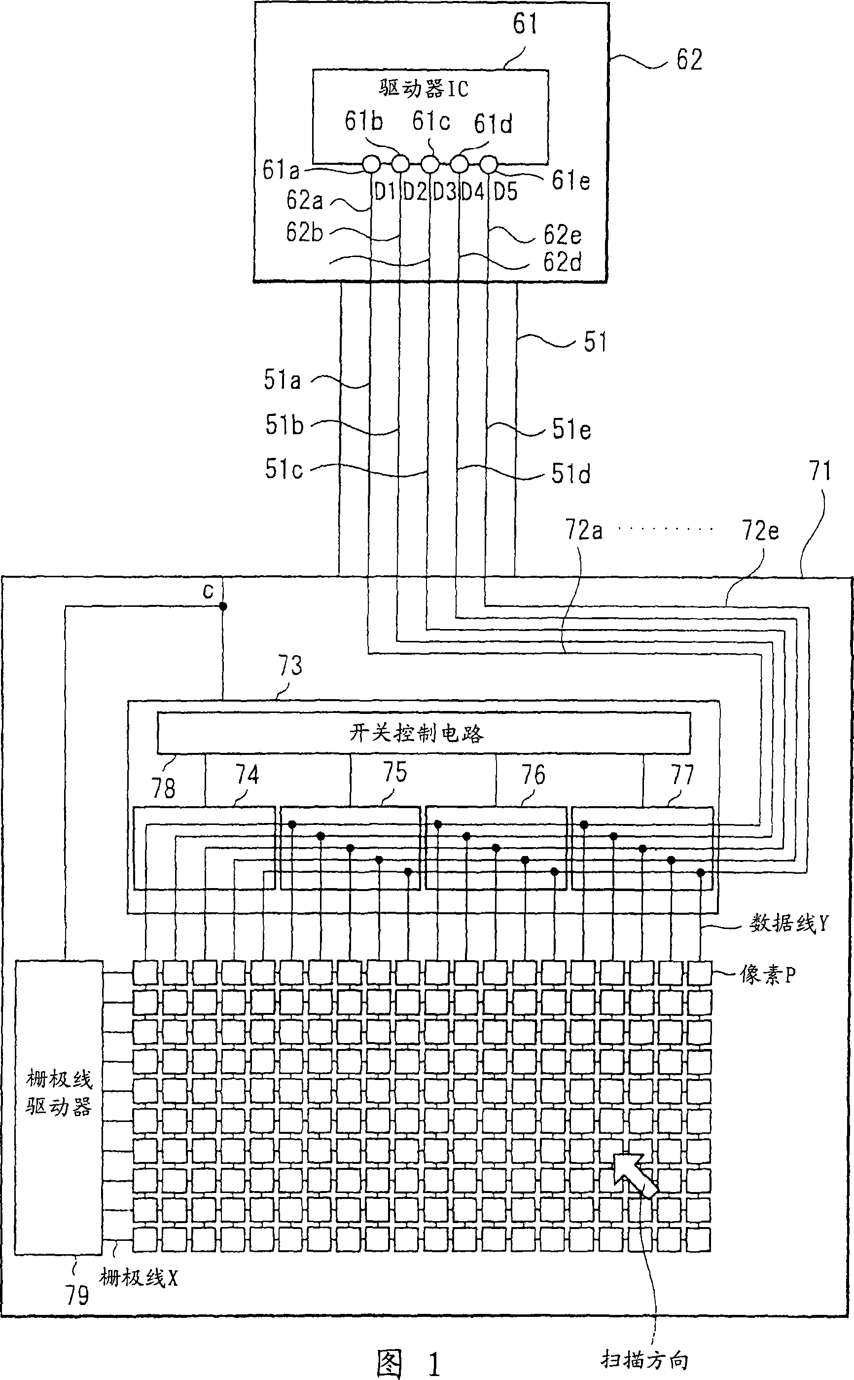
[0057] Hereinafter, a reflective liquid crystal display device having a dot sequential driving system to which an embodiment of the present invention is applied will be specifically described with reference to the accompanying drawings.

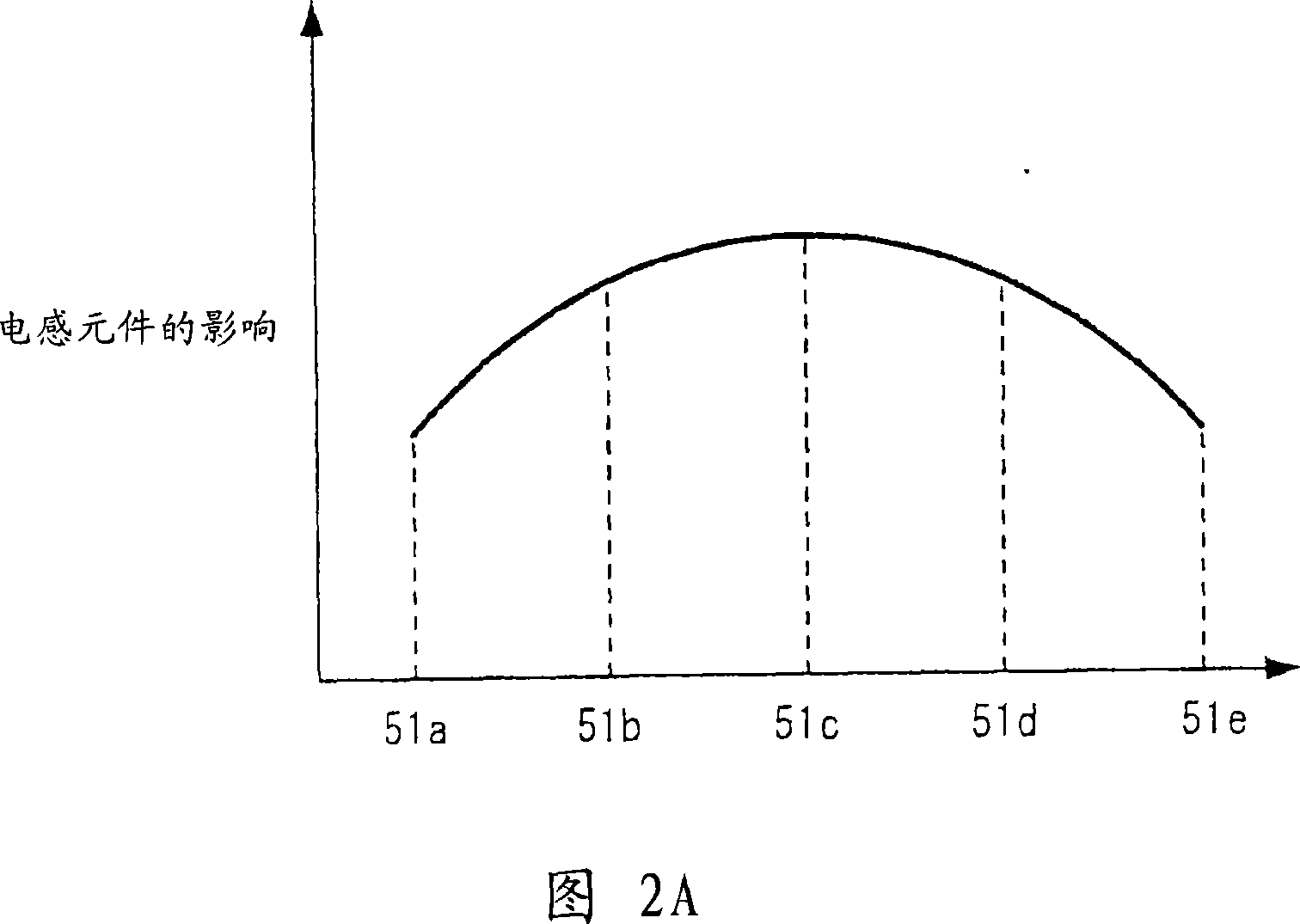
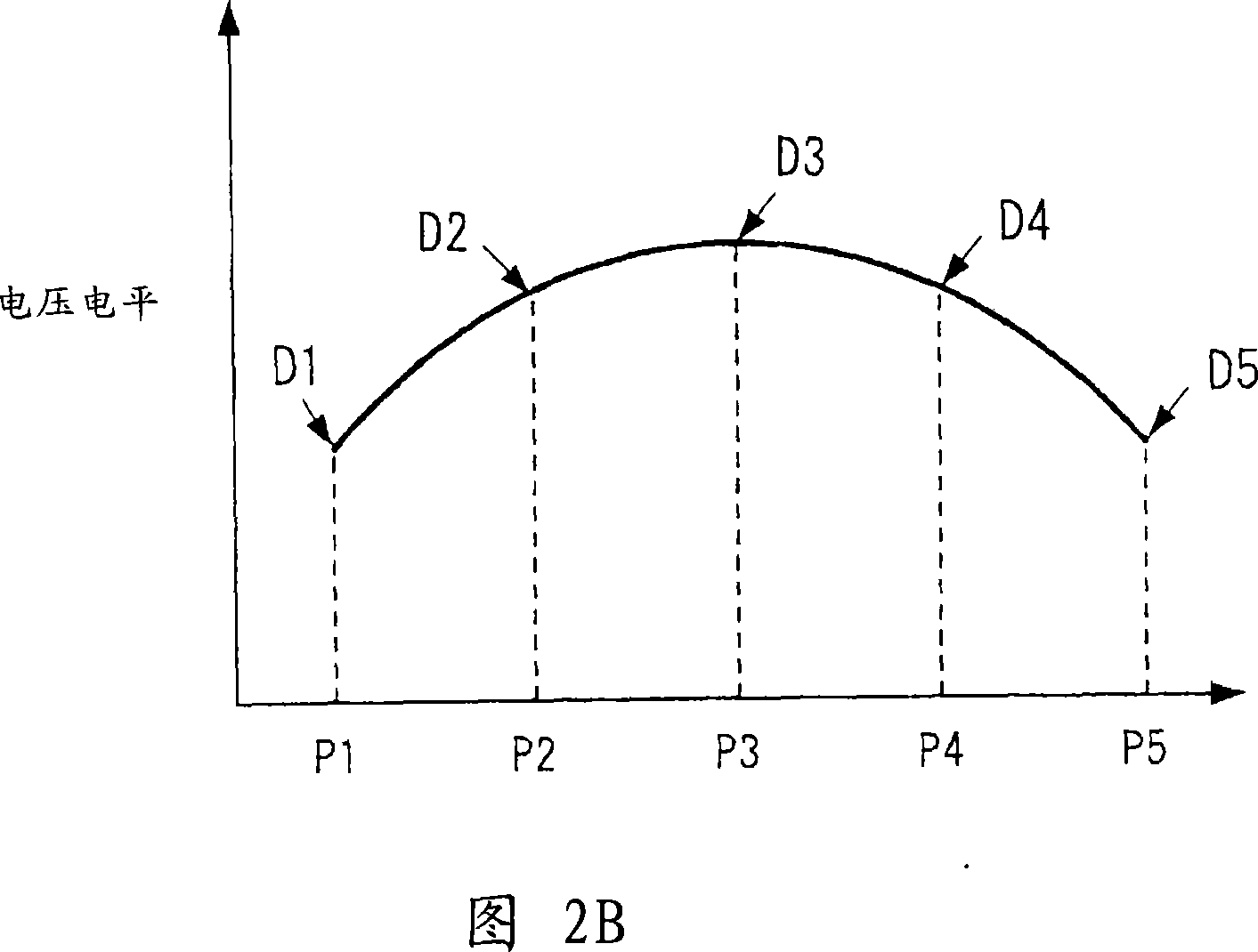
[0058] FIG. 4 is a diagram showing an example of an interconnect structure for a reflective liquid crystal display device having a dot sequential driving system to which an embodiment of the present invention is applied. In FIG. 4 , a driver IC 61 and a flexible printed circuit (FPC) 51 have the same structure as the driver IC 61 and FPC 51 shown in FIG. 1 . In addition, the FPC 51 includes two ground wires (for signal ground) at both ends.

[0059] In a reflective liquid crystal display device, gate lines X in the row direction and data lines Y in the column direction are arranged in a matrix form on a driving substrate 1 formed of a silicon substrate. Pixels (pixel drive circuits and pixel electrodes) P are arranged at intersections.

[0...


PUM


Abstract

An interconnect structure for a display device includes a driver from which display data are supplied, and an interconnect material having a plurality of signal lines disposed in parallel through which the display data are supplied from the driver. In the interconnect structure for a display device, the signal lines from which the display data are transmitted via the interconnect material are rearranged such that the display data via the signal lines having a comparatively larger effect of the inductance components and the display data via the signal lines having a comparatively smaller effect of the inductance components in the interconnect material are alternately supplied to adjacent pixels or groups of pixels of the display device. As a result, an image is displayed based on the luminance suitable for the display data.

Description

[0001] Cross References to Related Applications [0002] The present invention contains subject matter of Japanese Patent Application JP2006-009004 filed in Japan Patent Office on Jan. 17, 2006 and JP2006-336059 filed in Japan Patent Office on Dec. 13, 2006, the entire contents of which are hereby incorporated by reference. technical field [0003] The present invention relates to an interconnect structure for a display device externally connected to a driver. The invention also relates to a projection display device (projection system) applying the interconnection structure to an optical modulation device. Background technique [0004] In recent years, more attention has been paid to reflective devices that can reduce size, improve resolution, and exhibit high light utilization, and reflective devices have actually been used in projection systems with higher resolution and smaller size and higher brightness display device. The reflective device implies an active reflectiv...

Claims


Application Information

Patent Timeline
Patent Type & Authority Applications(China)
IPC IPC(8): G02F1/133G02F1/1362G09G3/36G03B21/00H04N9/31
Inventor 川浦英明形川晃一佐多博史
Owner SONY CORP
Why Eureka
Try Eureka