

Multi-domain vertical orientation mode liquid crystal display device and substrate manufacturing method thereof
A liquid crystal display device, a technology of vertical alignment mode, which is applied in the photoengraving process of the pattern surface, the manufacture of semiconductor/solid-state devices, optics, etc., and can solve the problems of color inconsistency, chromatic aberration, affecting the viewing angle range and picture quality, etc.
- Summary
- Abstract
- Description
- Claims
- Application Information
AI Technical Summary
Problems solved by technology
Method used
Image

Examples
Embodiment 1
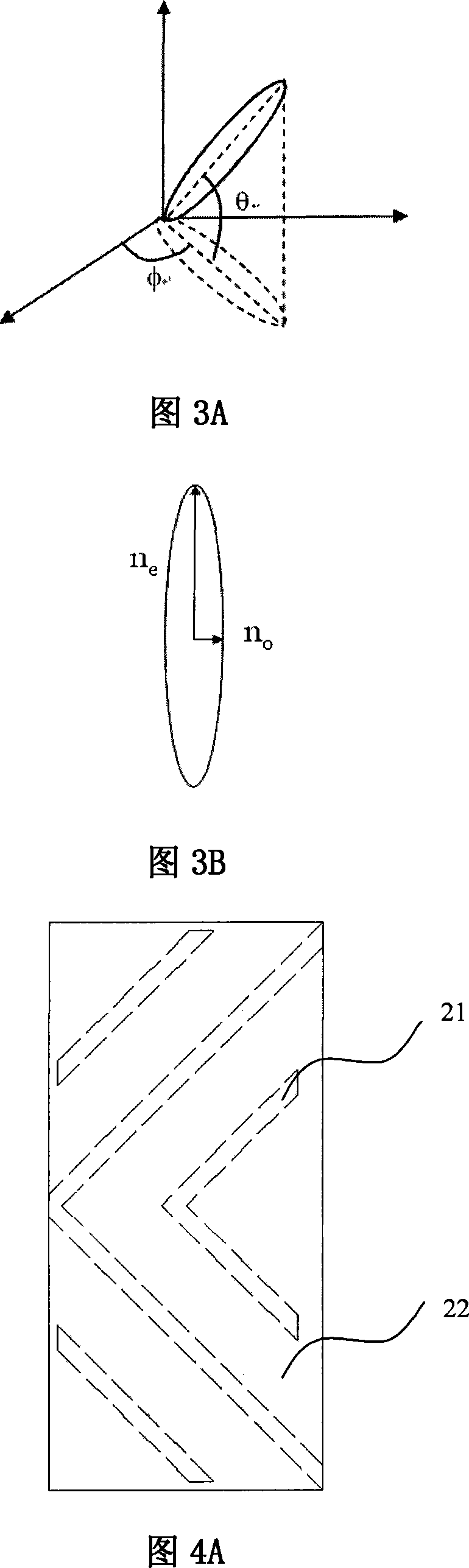
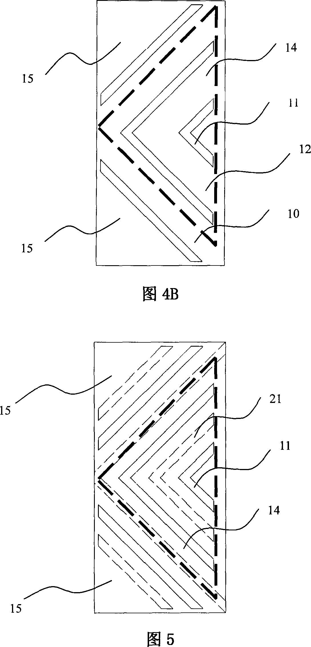
[0062] 4A is a schematic structural diagram of a common electrode on the upper substrate side in Embodiment 1 of the present invention; 4B is a schematic structural diagram of a pixel electrode in Embodiment 1 of the present invention.
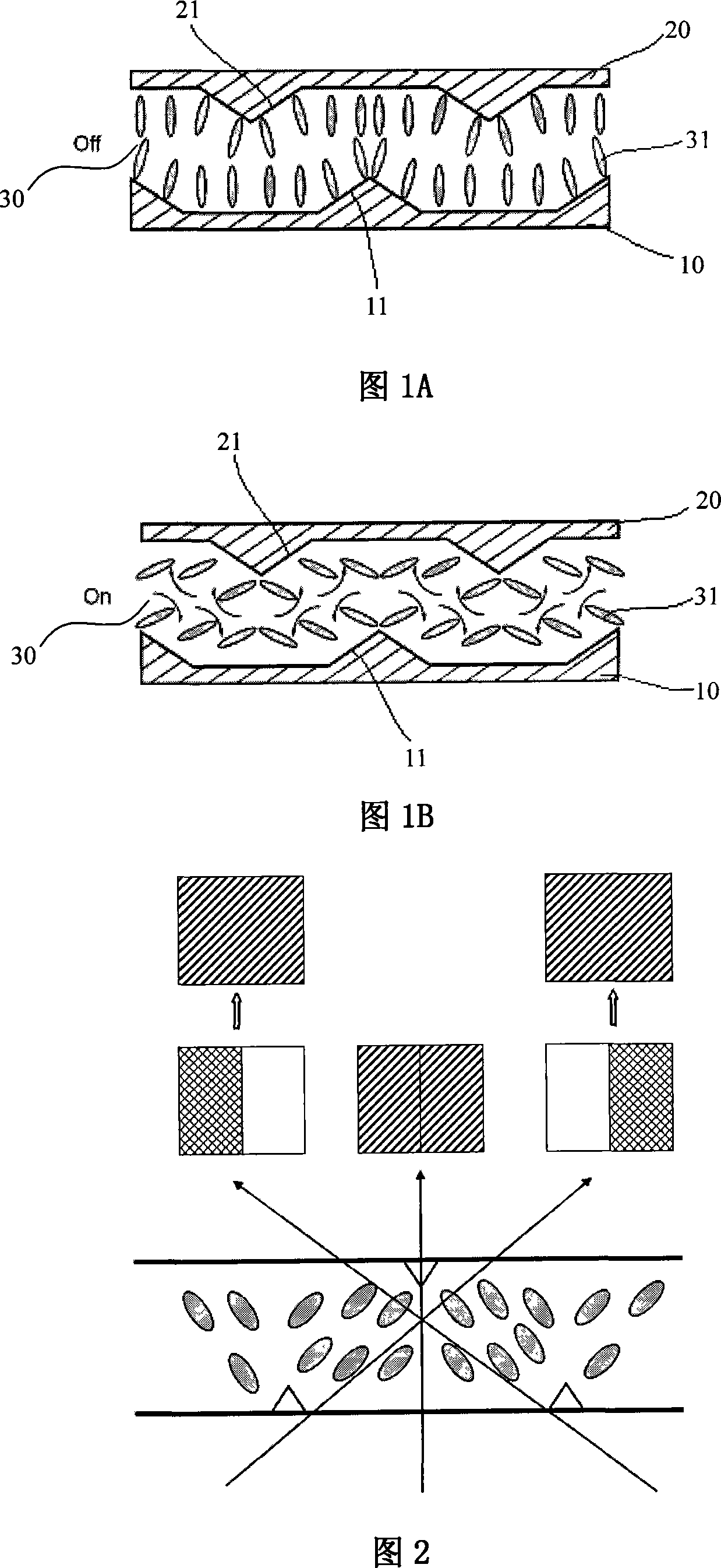
[0063] 4A, 4B, the liquid crystal display device of multi-domain vertical display mode of the present invention comprises an upper substrate 20, a lower substrate 10 and a liquid crystal layer 30 filled between the upper and lower substrates 10 and 20; the display area of the lower substrate 10 Contains a plurality of sub-pixel regions, pixel electrodes 12 and TFT devices (not shown in the figure) are arranged in the sub-pixels, slits or protrusions 11 are formed on the pixel electrodes 12; a common electrode 22 is formed on the surface of the upper substrate 20 , slits or protrusions 21 are formed on the common electrode 22 . The slit or protrusion 11 formed on the pixel electrode 12 is opposite to the slit or protrusion 21 on the common el...
Embodiment 2
[0074] FIG. 11 is a schematic diagram of the general manufacturing process and structure of the upper substrate.
[0075] Referring to Fig. 11A, first provide a transparent substrate 40, this transparent substrate 40 is a glass substrate or a plastic substrate; then form a black matrix (BM) 41 with a certain pattern on the transparent substrate 40, the material of BM41 can be made of black resin or metal chrome become. Referring to FIG. 11B , then, a color-resist layer 42 of a certain thickness is formed on the transparent substrate 40 with BM41, exposed using the mask plate 50 shown in FIG. 11C , and the pattern of the red color-resist layer after development is shown in FIG. 11D , repeating the manufacturing process shown in FIG. 11B to FIG. 11D to sequentially form red (R), green (G) and blue (B) color-resist layers as shown in FIG. 11E .
[0076] Again, a flat layer 43 with a certain thickness is formed on the three-layer color resist layer 42, as shown in FIG. 11F , the ...
Embodiment 3
[0081] In the process of using photolithography to manufacture the upper substrate 20, within the range of the sub-filter area, the color-resist layer 42 of the upper substrate 20 is prepared by using the micro-shift mask 53 and multiple exposures, so as to realize the same sub-filter area The thickness of the color resist layer 42 is different, for example, the thickness of the color resist in one part of the region is 2 microns, and the thickness of the color resist in another part of the region is 1.5 microns. The difference between the mask plate 53 of this embodiment and the traditional mask plate 50 is that the light-transmitting part of the mask plate 50 is the entire sub-filtering area, and the light-transmitting part of the mask plate 53 is 1 / 2 sub-filtering area. light area. Taking the red sub-filter area as an example, when forming the sub-filter area of the red color resist, firstly, 1 / 2 of the sub-filter area is exposed with the exposure amount X, and then the m...
PUM
| Property | Measurement | Unit |
|---|---|---|
| Thickness | aaaaa | aaaaa |
| Thickness | aaaaa | aaaaa |
Abstract
Description
Claims
Application Information