Display device
A display device and display panel technology, which is applied to static indicators, nonlinear optics, instruments, etc., can solve problems such as rising costs and increasing number of processes, and achieve the effect of reducing the number of manufacturing processes and reducing costs
- Summary
- Abstract
- Description
- Claims
- Application Information
AI Technical Summary
Problems solved by technology
Method used
Image

Examples
no. 1 approach
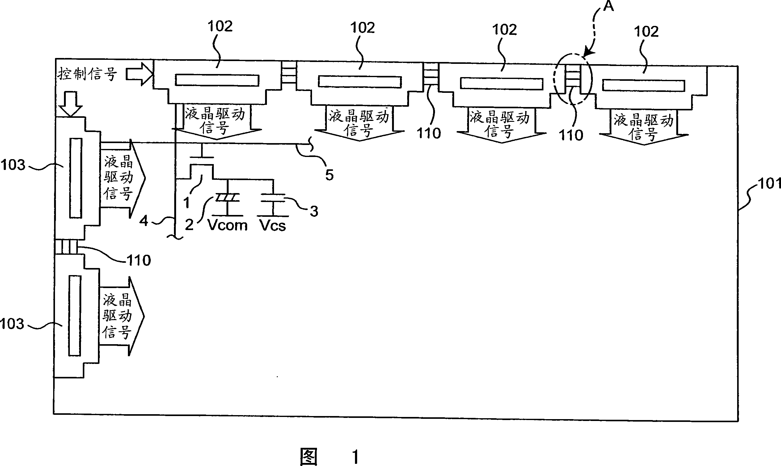
[0055] FIG. 1 is a schematic configuration diagram showing a first embodiment of a display device of the present invention. This display device includes a liquid crystal panel 101 as a display panel, a plurality of source-side drivers 102 as driving drivers, and a plurality of gate-side drivers 103 .
[0056] The plurality of source side drivers 102 are arranged in a straight line along one side of the liquid crystal panel 101 . The plurality of gate-side drivers 103 are arranged in a straight line along the other side intersecting with one side of the liquid crystal panel 101 .
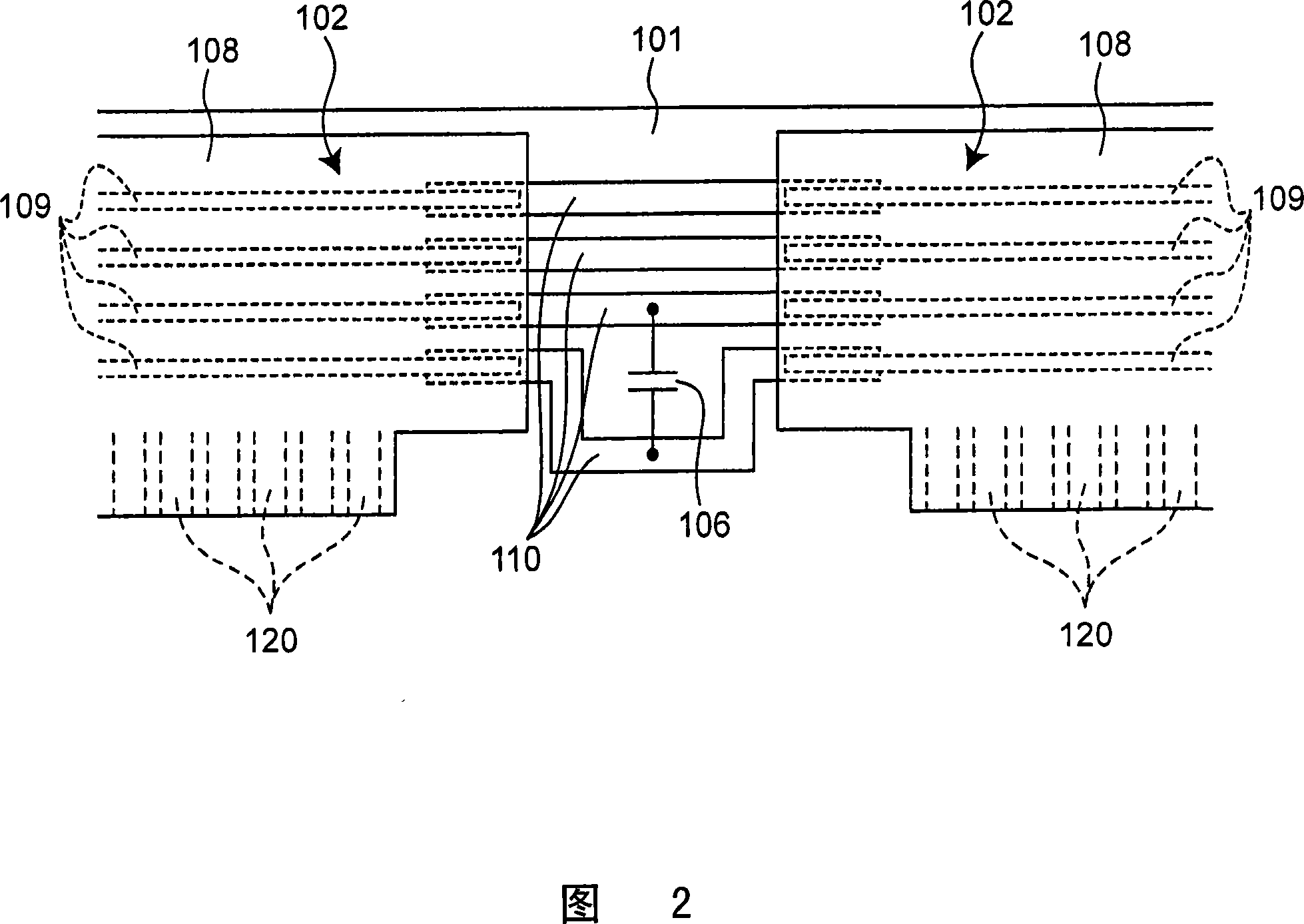
[0057] The panel-side wiring 110 is provided on the liquid crystal panel 101, and the panel-side wiring 110 is disposed between the adjacent source-side drivers 102, 102 and between the adjacent gate-side drivers 103, 103. At the same time, the signal lines of the adjacent source-side drivers 102 and 102 and the adjacent gate-side drivers 103 and 103 are electrically connected at the same time.
[...
no. 2 approach
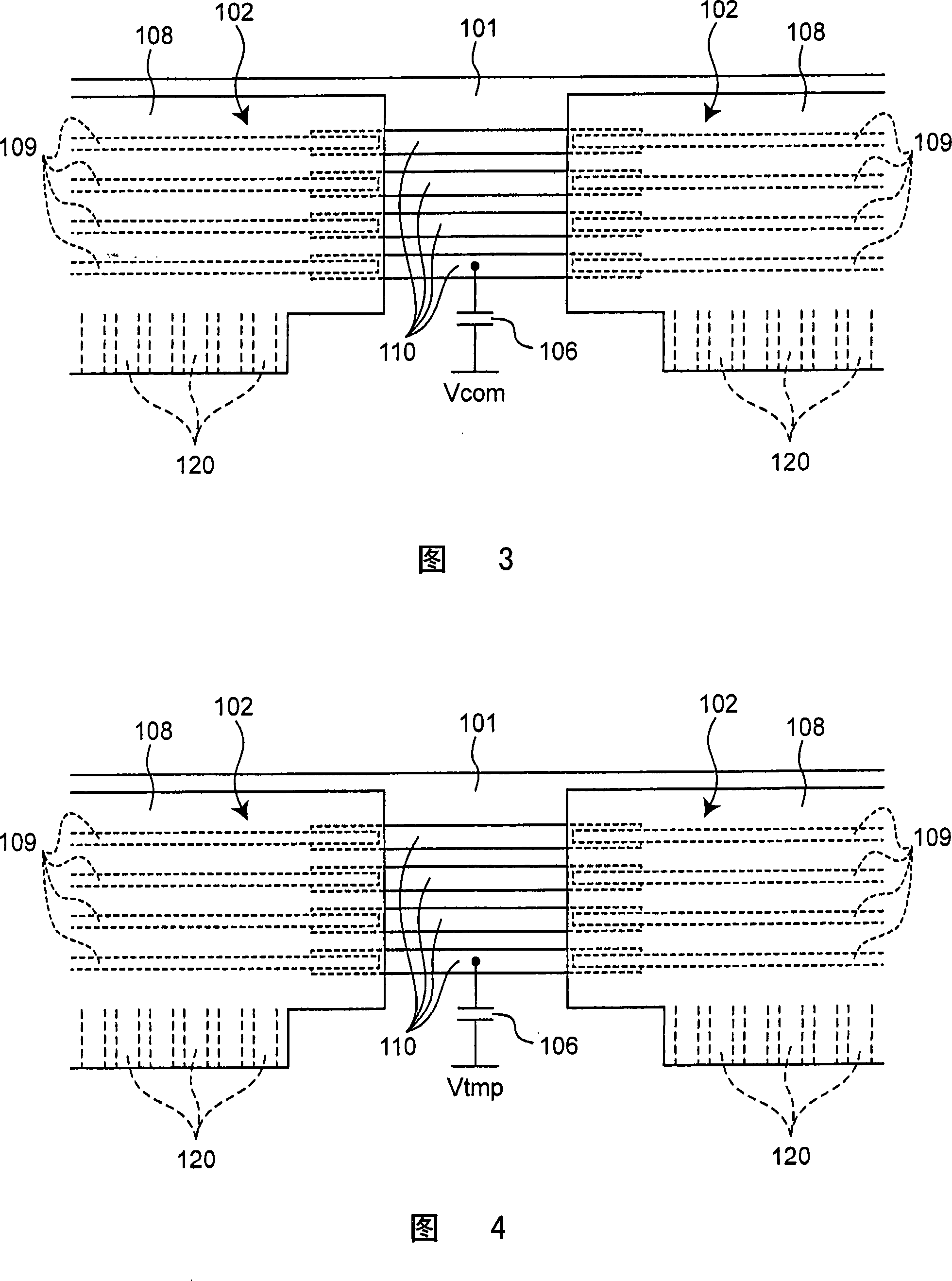
[0076] FIG. 3 shows a second embodiment of the display device of the present invention. The difference from the above-mentioned first embodiment (FIG. 2) will be described. In this second embodiment, one end of the capacitor 106 is connected to the panel-side wiring 110, and the other end of the capacitor 106 is connected to a common circuit formed on the liquid crystal panel 101. The electrodes Vcom are connected.
[0077] Specifically, the capacitor 106 is connected between the power supply wiring among the panel-side wiring 110 and the common electrode Vcom. That is, the capacitor 106 can be used as a bypass capacitor for preventing a voltage drop due to the influence of the impedance of the panel-side wiring 110 and the like.
[0078] In addition, the capacitor 106 may be arranged between the control signal wiring of the panel side wiring 110 and the common electrode Vcom, and the capacitor 106 may be used as an anti-interference for preventing interference of the control...
no. 3 approach
[0080] FIG. 4 shows a third embodiment of the display device of the present invention. In this third embodiment, one end of the capacitor 106 is connected to the panel-side wiring 110, and the other end of the capacitor 106 is connected to a portion to which an arbitrary voltage can be applied ( In this embodiment, the predetermined electrode Vtmp) is connected.
[0081] Specifically, the capacitor 106 is connected between the power supply line among the panel side lines 110 and the predetermined electrode electrode Vtmp. That is, the capacitor 106 can be used as a bypass capacitor for preventing a voltage drop due to the influence of the impedance of the panel-side wiring 110 and the like.
[0082] In addition, the capacitor 106 may be arranged between the control signal wiring of the panel side wiring 110 and the predetermined electrode Vtmp, and the capacitor 106 may be used as an anti-interference device for preventing interference of the control signal wiring. capacitor...
PUM
 Abstract
Description
Claims
Application Information