Mounting structure of electronic component

A technology for electronic components and mounting structures, which is applied in the direction of assembling printed circuits, electrical components, electrical components, etc., which can solve the problems of high cost, complex formation of insulating covering film 55, large insulating substrate 51, etc., and achieve narrow width Effect

Inactive Publication Date: 2007-12-26
ALPS ALPINE CO LTD
View PDF1 Cites 2 Cited by
  • Summary
  • Abstract
  • Description
  • Claims
  • Application Information

AI Technical Summary

Problems solved by technology

[0005] However, in the conventional electronic component mounting structure, since the underfill 56 is prevented from flowing out by the edge of the cover film removal portion 55a, in order to prevent the diffusion of the underfill 56, the insulating cover film 55 needs to be made thick film, in this case, the formation of the thick insulating cover film 55 becomes complicated and the cost becomes high
In addition, if the insulating cover film 55 is made into a thin film, in order to prevent the diffusion of the underfill 56, the cover film removal part 55a needs to be made wider. In this case, there is a problem that the insulating substrate 51 becomes larger.

Method used


Image

  • Mounting structure of electronic component
  • Mounting structure of electronic component
  • Mounting structure of electronic component

Examples


Embodiment Construction

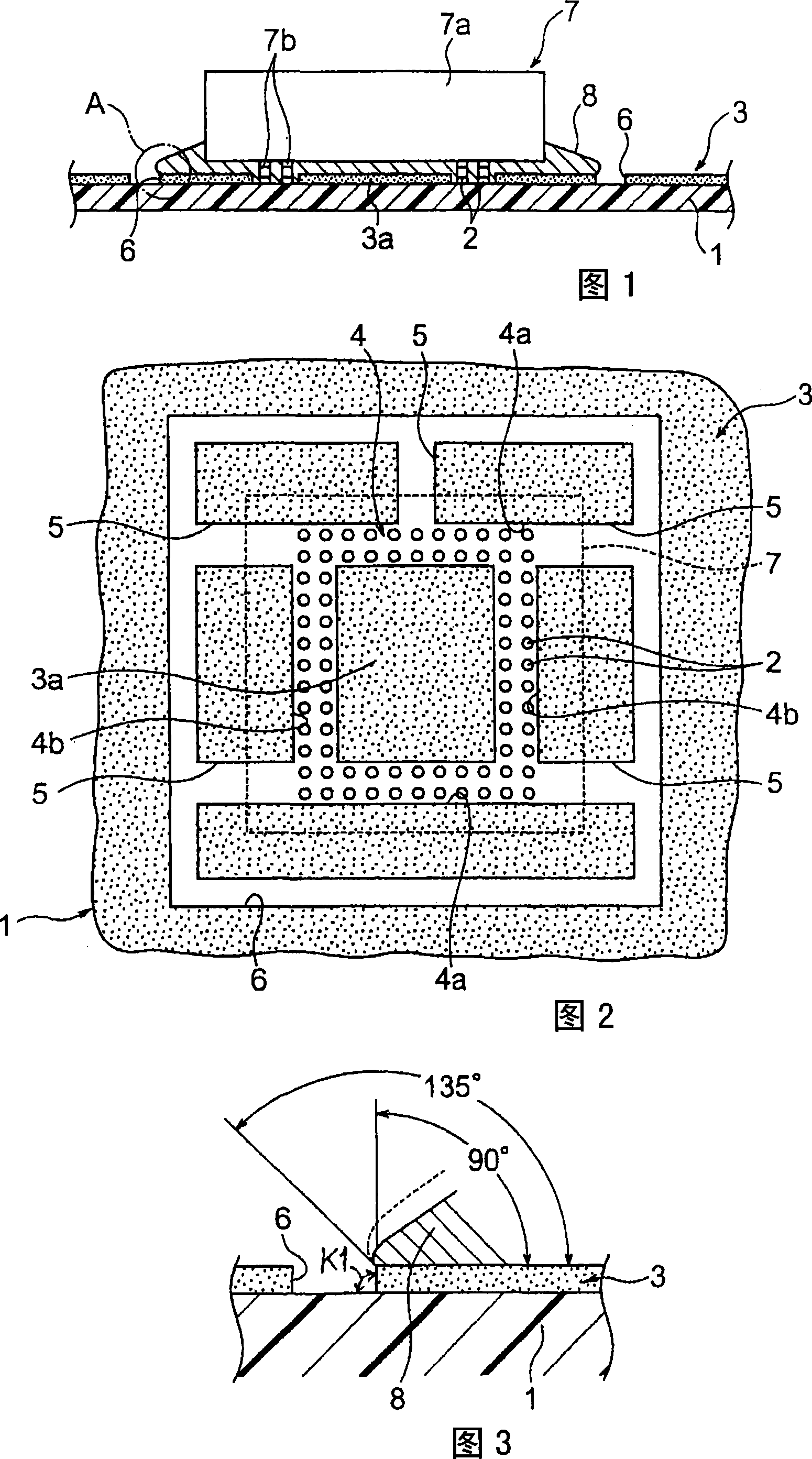
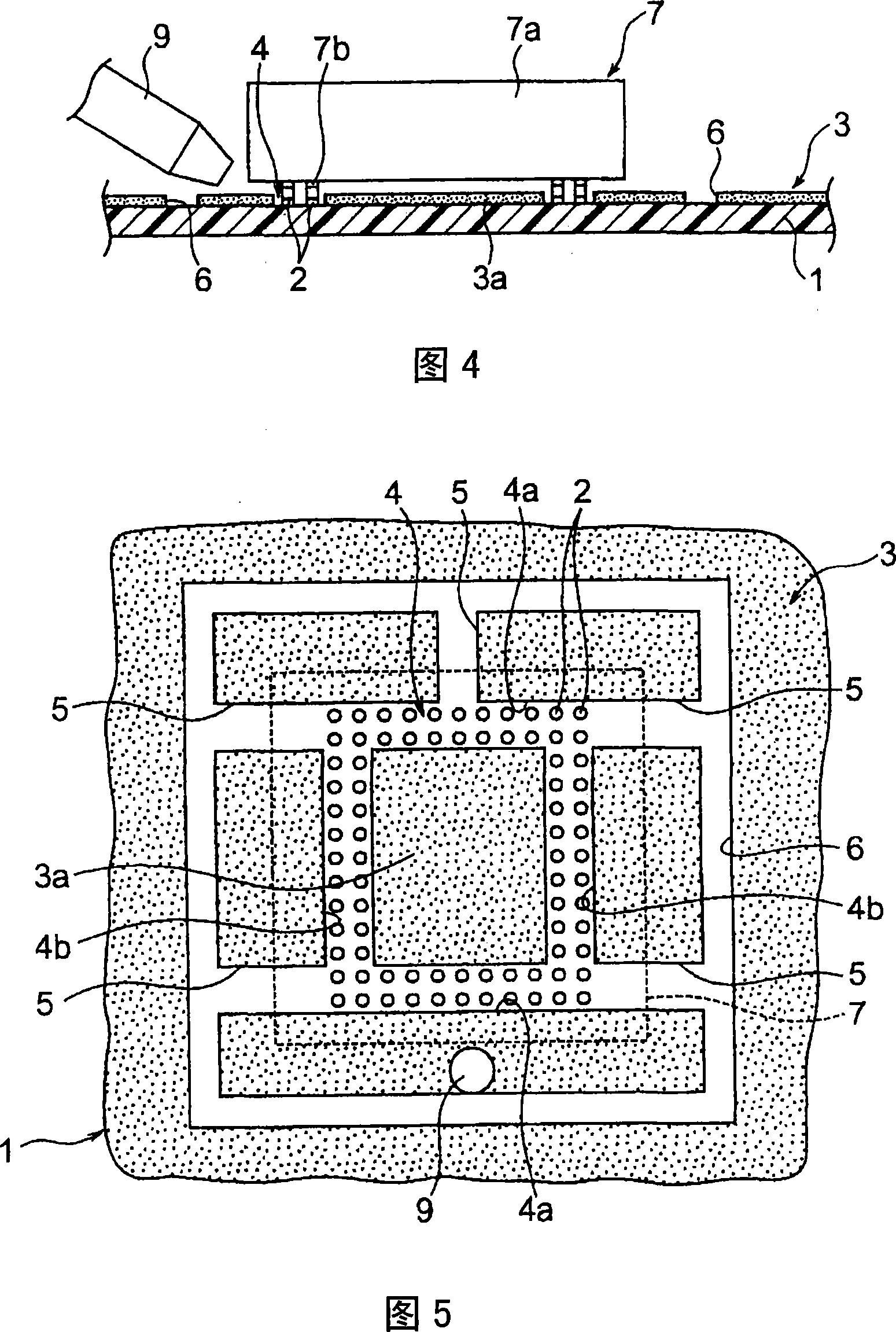
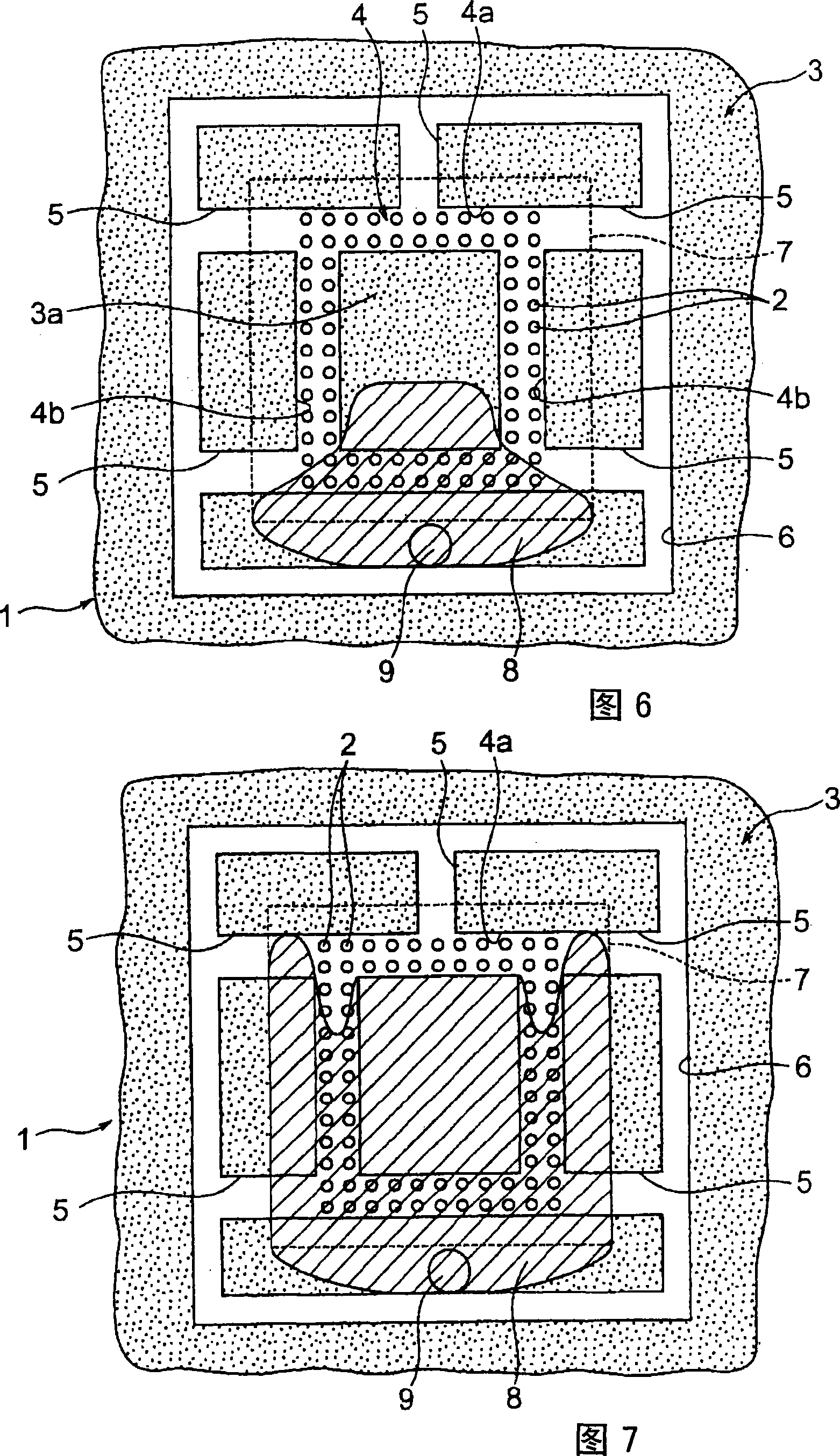
[0032] Hereinafter, embodiments of the invention will be described with reference to the drawings. 1 is a cross-sectional view of a main part of a mounting structure of an electronic component according to the present invention, FIG. 2 is a plan view of an insulating substrate of the mounting structure of an electronic component according to the present invention, FIG. 3 is an enlarged view of part A of FIG. 1 , and FIG. 4 It is a front view showing the mounting method of the electronic component of the present invention, FIG. 5 is a plan view showing the mounting method of the electronic component of the present invention, and FIG. 6 relates to the mounting method of the electronic component of the present invention and shows a liquid underfill In the explanatory diagram of the first flow state of the glue, FIG. 7 relates to the mounting method of the electronic component of the present invention, and is an explanatory diagram showing the second flow state of the liquid underf...


PUM


Abstract

To provide a low-cost mounting structure of electronic component with a small size where the spreading of underfill on an insulating coat is suppressed by a film removing portion. In the mounting structure of the electronic components, spreading of the underfill 8, prepared on the insulating coat 3, is controlled by the coat exception portion 6, and the spreading of the underfill 8 beyond it does not exist. Since the suppression effects of the spreading of the underfill 8 is not relevant to the thickness, the depth and the width of the film removing portion 6, the film removing portion 6 can be made thin, shallow and narrow, and low cost, and thus miniaturization and thinning of an insulating substrate 1 can be facilitated.

Description

technical field [0001] The present invention relates to a mounting structure of electronic components suitable for various electronic devices, electronic circuit units, and the like. Background technique [0002] Fig. 16 is an explanatory diagram showing a conventional mounting structure of an electronic component when describing a drawing related to a conventional mounting structure of an electronic component. Next, the configuration of a conventional electronic component mounting structure will be described with reference to FIG. 16 . The electronic component 54 is mounted on the circuit pattern 52 provided on the insulating substrate 51 via bumps 53 . [0003] In addition, an insulating cover film 55 is provided on the insulating substrate 51 and the circuit pattern 52 except for the area of ​​the electronic component 54. The insulating cover film 55 is configured as follows: a cover film removal portion is provided at a position including the area of ​​the electronic co...

Claims


Application Information

Patent Timeline
Patent Type & Authority Applications(China)
IPC IPC(8): H01L23/488H01L23/498H01L23/31
CPCH01L2224/73204H01L2224/16225H01L2224/26175H01L2224/32225H01L2924/00012H05K3/30H05K13/04
Inventor 千寻和夫本间友幸
Owner ALPS ALPINE CO LTD
Why Eureka
Try Eureka