
Scan chain and method that realizing high speed testing circuitry

A scan chain and circuit technology, applied in the field of scan chain circuits, can solve the problem of not providing scanning capabilities

Active Publication Date: 2008-01-02
GLOBALFOUNDRIES INC
View PDF0 Cites 23 Cited by
  • Summary
  • Abstract
  • Description
  • Claims
  • Application Information

AI Technical Summary

Problems solved by technology

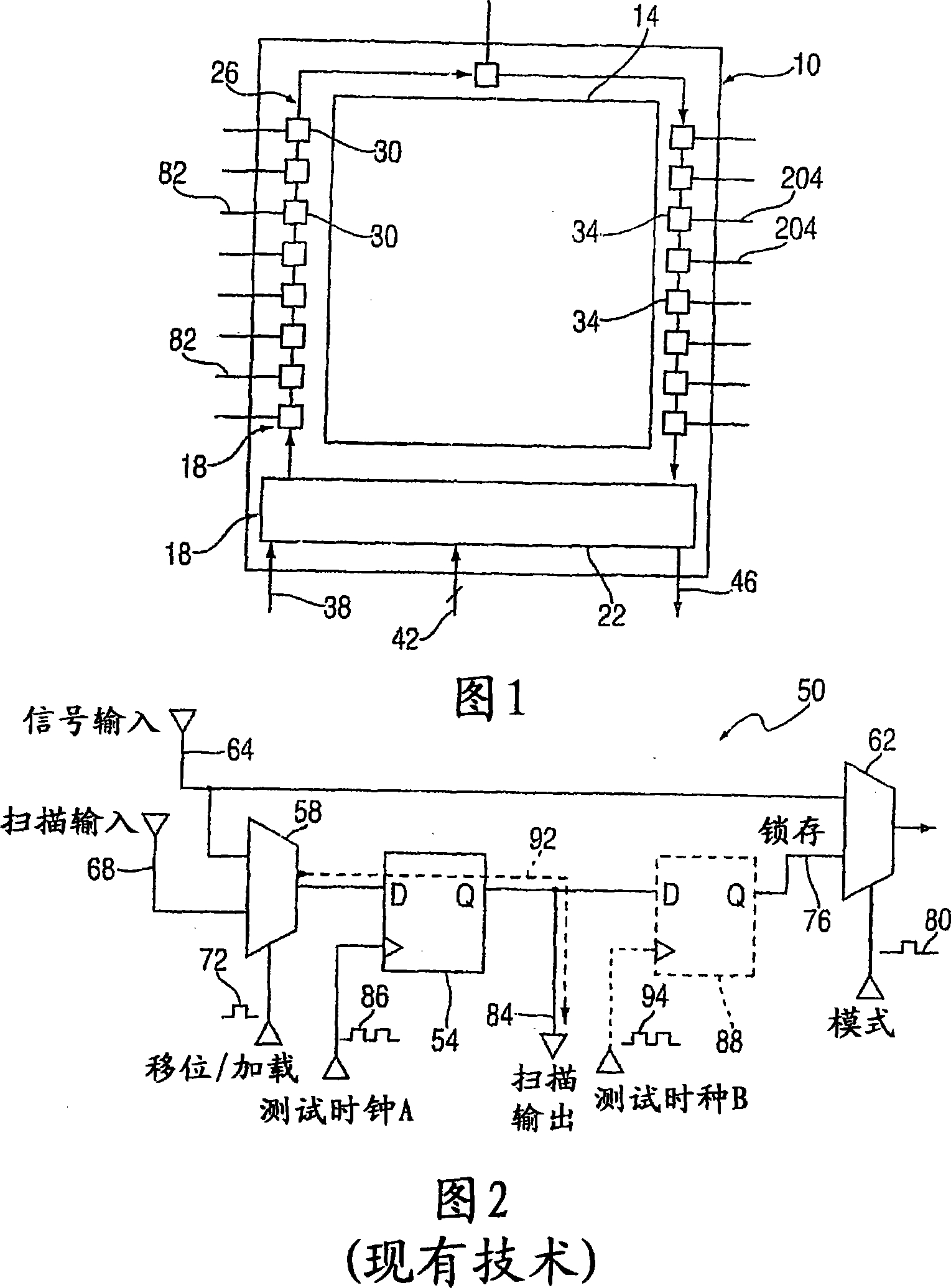
One disadvantage of conventional boundary-scan circuits is that they do not provide a convenient way to scan functional circuits (e.g., core logic) at their normal operating functional speeds using the scanning capabilities of scan circuit structures such as scan circuit structure 18 of FIG. ) method for performing transition delay test

Method used


Image

  • Scan chain and method that realizing high speed testing circuitry
  • Scan chain and method that realizing high speed testing circuitry

Examples


Embodiment Construction

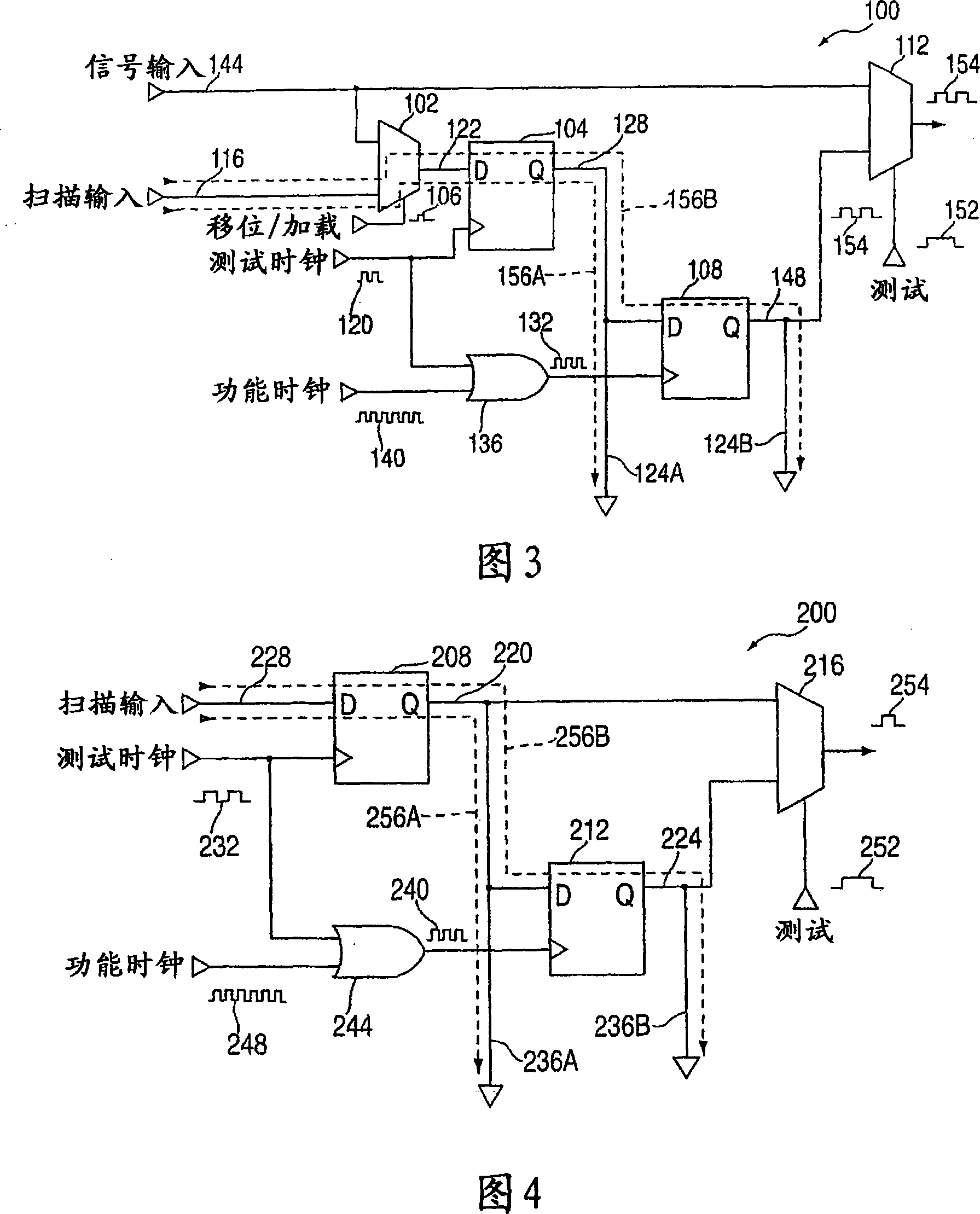
[0014] FIG. 3 shows a scan unit 100 of the present invention that can be used in a scan circuit, such as the boundary scan circuit structure 18 of FIG. 1 . The scan unit 100 of FIG. 3 is unique in that it allows a functional circuit (such as the core logic 14 of FIG. 1 , located on the same integrated circuit (IC) chip, such as IC chip 10 ) to operate as a scan unit at the normal operating functional speed of the circuit. The unit is transition delay tested. That is, scanning unit 100 is configured to provide functional circuitry with one or more "toggle" transitions (e.g., 1→0, 0→1, 1→0→1, 0→1→0, etc.) transition delay test data in order to test the high-speed integrity of the circuit. This function speed is usually much faster than the typical scan speed of 50MHz to 125MHz, and may be in the gigahertz range.

[0015] The scanning unit 100 may include a first multiplexer (MUX) 102, a first scanning register (eg, a flip-flop or a latch) 104, a second scanning register (eg, a...


PUM


Abstract

Boundary scan circuitry that includes a plurality of scan cells that each contain two scan registers each for storing a respective test value. During on-chip or inter-chip testing, one of the scan registers is responsive to a functional clock signal so that the test cell generates transition delay test data having at least one state transition made at the speed of the functional clock signal. The transition delay test data allows the integrity of on-chip functional circuitry or the integrity of inter-chip circuitry to be verified at full functional speed.

Description

technical field [0001] The present invention generally relates to the field of integrated circuits. The invention is particularly directed to scan chain circuits that enable scan testing at functional clock speeds. Background technique [0002] Conventional integrated circuit (IC) scan testing has two main functions. First, in a multi-chip environment, scan testing allows verification of the integrity of inter-die connections. This type of scan testing is commonly referred to as "boundary scan" testing and is the subject of Institute of Electrical and Electronics Engineers (IEEE) Standard 1149.1, the entire contents of which are hereby incorporated by reference for background and contextual information. Second, in a single-chip environment, scan testing allows the functional blocks of an integrated circuit to be isolated from external pins as described in the 1149.1 standard, or boundary-scan around the circuit core inside the chip in the case of the IEEE1500 standard unde...

Claims


Application Information

Patent Timeline
Patent Type & Authority Applications(China)
IPC IPC(8): G01R31/3181G01R31/317
CPCG01R31/318552G01R31/318536
Inventor 格雷·D.·格里斯马克·R.·泰勒斯蒂文·F.·奥克兰
Owner GLOBALFOUNDRIES INC
Learn More