Method for manufacturing semiconductor integrated circuit device

A technology of integrated circuits and manufacturing methods, which is applied in semiconductor/solid-state device manufacturing, semiconductor devices, circuits, etc., and can solve problems such as adverse effects of photoelectric conversion of photodetectors and uneven incident efficiency

Inactive Publication Date: 2008-01-23
SANYO ELECTRIC CO LTD +1
View PDF1 Cites 0 Cited by
  • Summary
  • Abstract
  • Description
  • Claims
  • Application Information

AI Technical Summary

Problems solved by technology

[0013] In this way, when the bottom surface of the opening 15 is formed unevenly, the incidence efficiency in the surface of the light receiving part 11 is not uniform.
In addition, the unevenness of the bottom surface of the opening 15 reflects light, which may adversely affect the photoelectric conversion of the photodetector.

Method used


Image

  • Method for manufacturing semiconductor integrated circuit device
  • Method for manufacturing semiconductor integrated circuit device
  • Method for manufacturing semiconductor integrated circuit device

Examples


Embodiment Construction

[0023] Embodiments of the present invention will be described below with reference to the drawings.

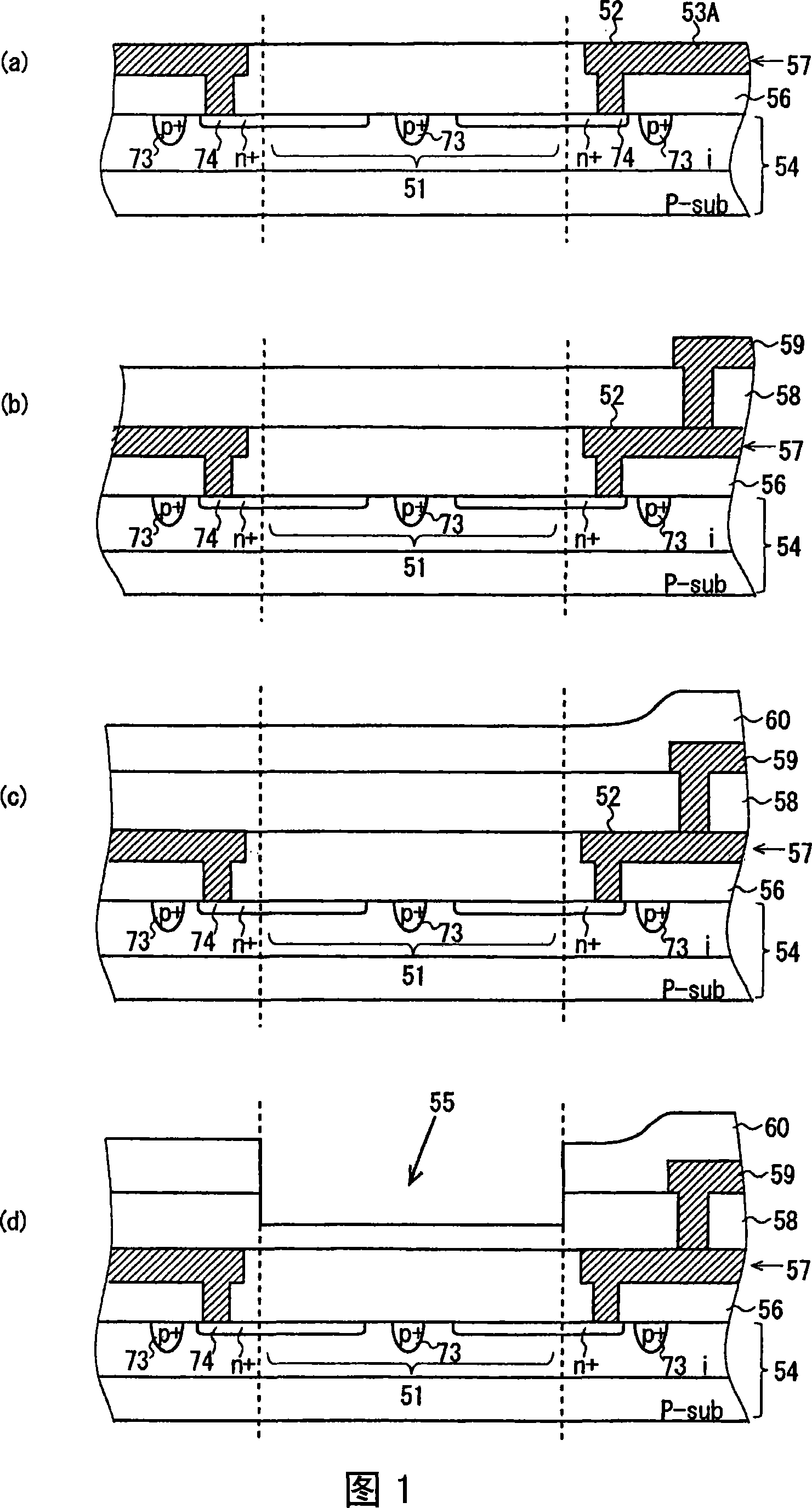
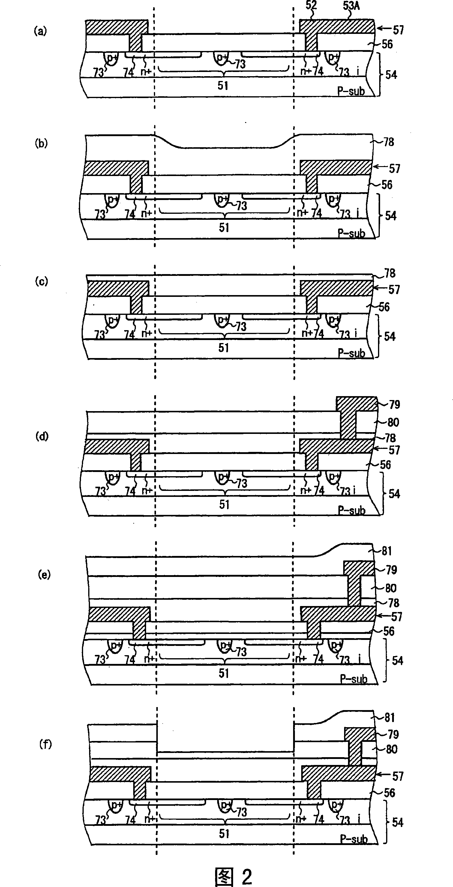
[0024] FIG. 1 is a diagram showing a photodetector formation process of Example 1. FIG.

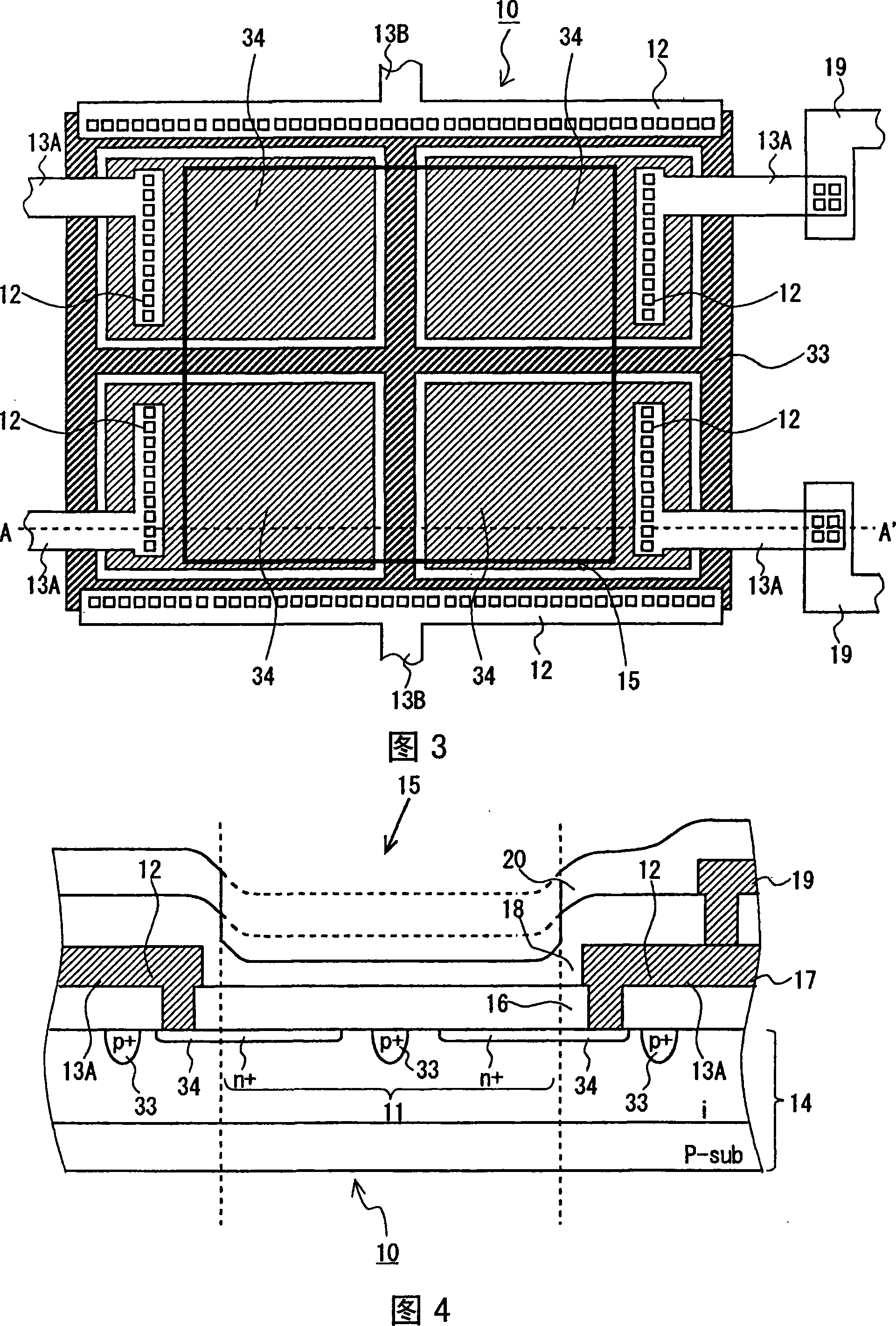
[0025] Fig. 1 shows a section through the line A-A' shown in Fig. 3 and perpendicular to the semiconductor substrate. In addition, the planar shape of the photodetector in this embodiment is the same as that in FIG. 3 .

[0026] First, a first insulating film 56 is formed on a semiconductor substrate 54 on which a light receiving portion 51 has been formed, and a first metal layer 57 is formed by a damascene method ( FIG. 1( a )). The first metal layer 57 is formed of aluminum (Al), tungsten (W), or the like. The surfaces of the first insulating film 56 and the first metal layer 57 are formed flat by the damascene method, and the wiring structure 52, the signal line 53A connecting the wiring structure 52, and the voltage application line (not shown) are formed on the first metal layer 5...


PUM


Abstract

Due to a difference in a film thickness generated in structure layers located on top of a light receiver, a bottom surface of an open part does not flatten and an amount of incident light within a surface of the light receiver becomes nonuniform. A flat layer is formed by using a damascene process to form a first metal interlayer or by polishing using CMP an insulation film stacked after the first metal layer is formed. As a result, the insulation film stacked on the light receiver is also formed evenly. Thus, when an inside of the light receiver is opened by etching, the bottom surface of the open part can be formed evenly.

Description

technical field [0001] The present invention relates to a semiconductor integrated circuit device in which an integrated circuit is formed on a semiconductor substrate including a light receiving portion, and more particularly to a method of manufacturing a semiconductor integrated circuit device in which an opening is formed by etching an interlayer insulating film stacked on the substrate. Background technique [0002] In recent years, optical discs such as CDs (Compact Disks) and DVDs (Digital Versatile Disks) occupy a large place as information recording media. These optical disc playback devices reproduce recorded data based on detection of changes in the intensity of reflected light of laser light irradiated along the tracks of the optical disc by a photodetector. [0003] FIG. 3 is a schematic plan view of a conventional photodetector 10 . [0004] FIG. 4 is a schematic cross-sectional view showing the light-receiving portion 11 and the wiring structure 12 on a cross...

Claims


Application Information

Patent Timeline
Patent Type & Authority Applications(China)
IPC IPC(8): H01L21/768H01L21/3105
CPCH01L31/18H01L31/02002H01L31/105
Inventor 野村洋治
Owner SANYO ELECTRIC CO LTD
Why Eureka
Try Eureka