A camera module of curved surface cmos image sensor

An image sensor and camera module technology, applied in image communication, instruments, televisions, etc., can solve the problems of poor image quality at the edge of the image, reduce the reflection of incident light, shorten the flange focal length, etc., to reduce the size, improve the overall performance, The effect of shortening the flange focal length

Active Publication Date: 2018-01-26
SHANGHAI INTEGRATED CIRCUIT RES & DEV CENT +1
View PDF6 Cites 0 Cited by
  • Summary
  • Abstract
  • Description
  • Claims
  • Application Information

AI Technical Summary

Problems solved by technology

[0014] The purpose of the present invention is to overcome the above-mentioned defects of poor portability and poor imaging quality of the image edge in the prior art, and provide a curved surface CMOS image sensor camera module, which uses a double Gaussian lens without spherical aberration correction mirror as The main lens, the opposite surface of the CMOS image sensor facing the main lens is designed as a concave curved surface corresponding to the main lens, and the incident light is transmitted through an optical fiber coupled with a color filter, so that the main lens is simplified and the flange focal length is shortened. Effectively reduce the reflection of incident light, improve photosensitivity, and improve the overall image quality while reducing the size of the module

Method used


Image

  • A camera module of curved surface cmos image sensor
  • A camera module of curved surface cmos image sensor
  • A camera module of curved surface cmos image sensor

Examples


Embodiment 1

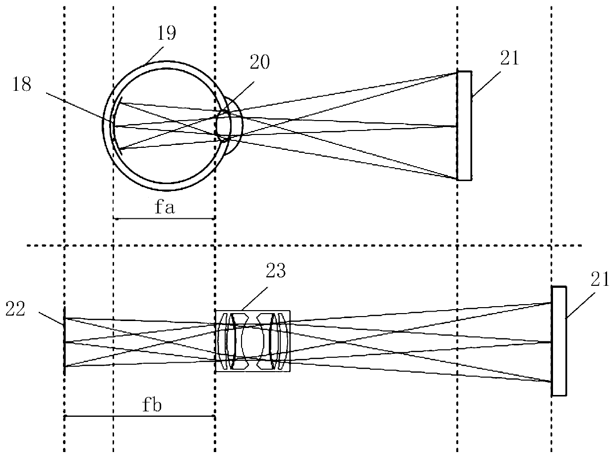
[0044] In this example, see Figure 5 , Figure 5 It is a schematic cross-sectional view of the camera module of the curved surface CMOS image sensor in Embodiment 1 of the present invention. Such as Figure 5 As shown, the curved surface CMOS image sensor camera module of the present invention includes two components of a coupled main lens 46 and a CMOS image sensor 35 . The main lens 46 is based on the double Gauss lens, but the spherical aberration correction lens is canceled. Therefore, the number of lenses is reduced by 3 compared to a typical double Gauss lens composed of 6 lenses, which includes a first convex lens 45 , a concave lens 44 , and a second convex lens 43 from top to bottom. Wherein, the first convex lens 45 and the second convex lens 43 are single-convex lenses, and their convex surfaces are set facing the outer direction of the main lens 46 group, and the concave lens 44 is a double-concave lens. After the main lens 46 cancels the spherical aberration ...

Embodiment 2

[0054] In this example, see Figure 6 , Figure 6 It is a schematic cross-sectional view of the camera module of the curved surface CMOS image sensor in the second embodiment of the present invention. Such as Figure 6 As shown, the curved surface CMOS image sensor camera module of the present invention includes two components of a coupled main lens 46 and a CMOS image sensor 49 . The design of the main lens 46 is exactly the same as that of Embodiment 1 (therefore, the same numerals are used), and it is also based on a double Gauss lens, but the spherical aberration correction lens is canceled, and the number of lenses is also 3. The main lens 46 sequentially includes a first convex lens 45 , a concave lens 44 , and a second convex lens 43 from top to bottom. Wherein, the first convex lens 45 and the second convex lens 43 are single-convex lenses, and their convex surfaces are set facing the outer direction of the main lens 46 group, and the concave lens 44 is a double-con...

Embodiment 3

[0063] In this example, see Figure 7 , Figure 7 It is a schematic cross-sectional view of the camera module of the curved surface CMOS image sensor in the third embodiment of the present invention. Such as Figure 7 As shown, this embodiment is another implementation manner of the first embodiment. The difference between this embodiment and Embodiment 1 is that the surface of the concave curved surface 40 of the metal layer 47 of the sensor 35 has the same curvature as the convex surface of the second convex lens 43 of the main lens 46, namely The shape of the concave curved surface 40 completely matches the convex shape of the second convex lens 43 of the main lens 46 . Therefore, the concave curved surface 40 and the second convex lens 43 are closely coupled, and there is no gap at all. That is to say, at this moment, the flange focal length of the main lens 46 is zero. Correspondingly, the upper end of the optical fiber 39 is no longer exposed, but is indented into t...


PUM


Abstract

The invention discloses a camera module of a curved surface CMOS image sensor. By adopting a double Gaussian lens without a spherical aberration correction mirror as the main lens, the opposite surface of the sensor facing the main lens is designed as a concave curved surface corresponding to the main lens, and Couple the two ends of the optical fiber coupled with the color filter to the photodiode and the main lens to transmit the incident light, so that the incident light derived from the main lens can diverge into each optical fiber, and then reach the photodiode after being restored by the color filter , can effectively eliminate the reflection of incident light and the crosstalk between pixels, improve the photosensitivity, realize the improvement of the overall image quality while reducing the size of the module.

Description

technical field [0001] The invention relates to the field of integrated circuits, more specifically, to a camera module with a curved surface CMOS image sensor that can improve photosensitivity and simplify the main lens. Background technique [0002] A CMOS image sensor camera module in the prior art includes two components: a CMOS image sensor and a main lens. [0003] Image sensors are devices that convert optical signals into electrical signals, and have been widely used in civil and commercial fields such as digital TV and visual communication. According to different photoelectric conversion methods, image sensors can generally be divided into two types: charge-coupled device image sensor (Charge-coupled Device, CCD) and CMOS image sensor (CMOS IMAGE SENSOR, CIS). [0004] For CCDs, on the one hand, in professional scientific research and industrial fields, CCDs with high signal-to-noise ratio are the first choice; on the other hand, in the field of high-end photograph...

Claims


Application Information

Patent Timeline
Patent Type & Authority Patents(China)
IPC IPC(8): H04N5/225G02B13/00
Inventor 陈嘉胤
Owner SHANGHAI INTEGRATED CIRCUIT RES & DEV CENT
Why Eureka
Try Eureka