Semiconductor device and method for manufacturing same

一种半导体、器件的技术,应用在半导体器件及其制造领域,能够解决难以具有较大截面积等问题

Inactive Publication Date: 2008-01-30
PANASONIC CORP
View PDF2 Cites 14 Cited by
  • Summary
  • Abstract
  • Description
  • Claims
  • Application Information

AI Technical Summary

Problems solved by technology

[0010] However, in the case of wiring at a narrow pitch, the width of the wiring itself is required to be narrowed. Therefore, even if the low-melting-point metal layer is raised as described above, it is difficult to have a large cross-sectional area.

Method used


Image

  • Semiconductor device and method for manufacturing same
  • Semiconductor device and method for manufacturing same
  • Semiconductor device and method for manufacturing same

Examples


Embodiment Construction

[0040] Hereinafter, embodiments of the present invention will be described with reference to the drawings.

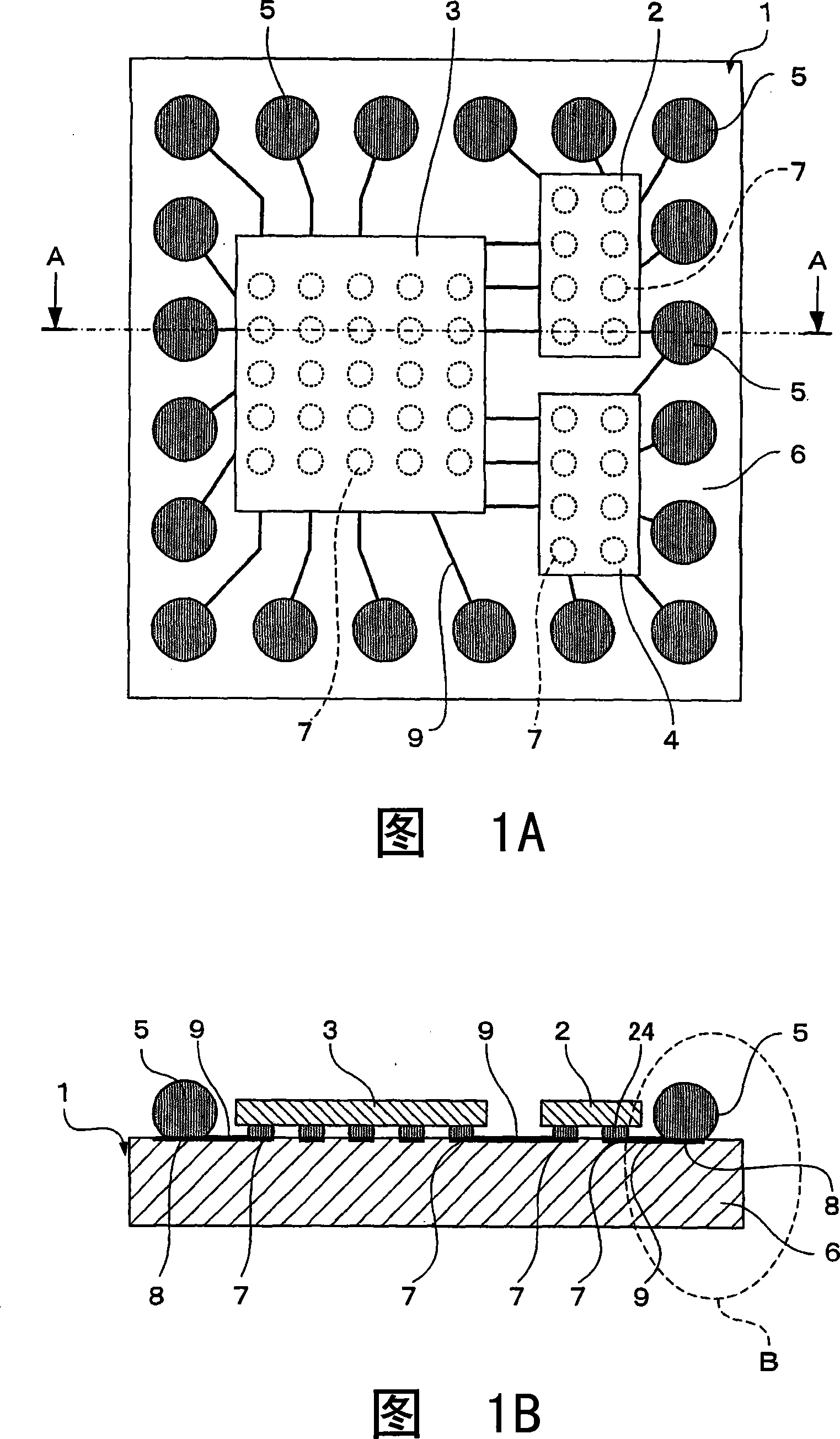
[0041] The semiconductor device shown in Fig. 1 and Fig. 2 has: wiring substrate 1; IC chips 2, 3, 4; Understand that shown is less than actual).

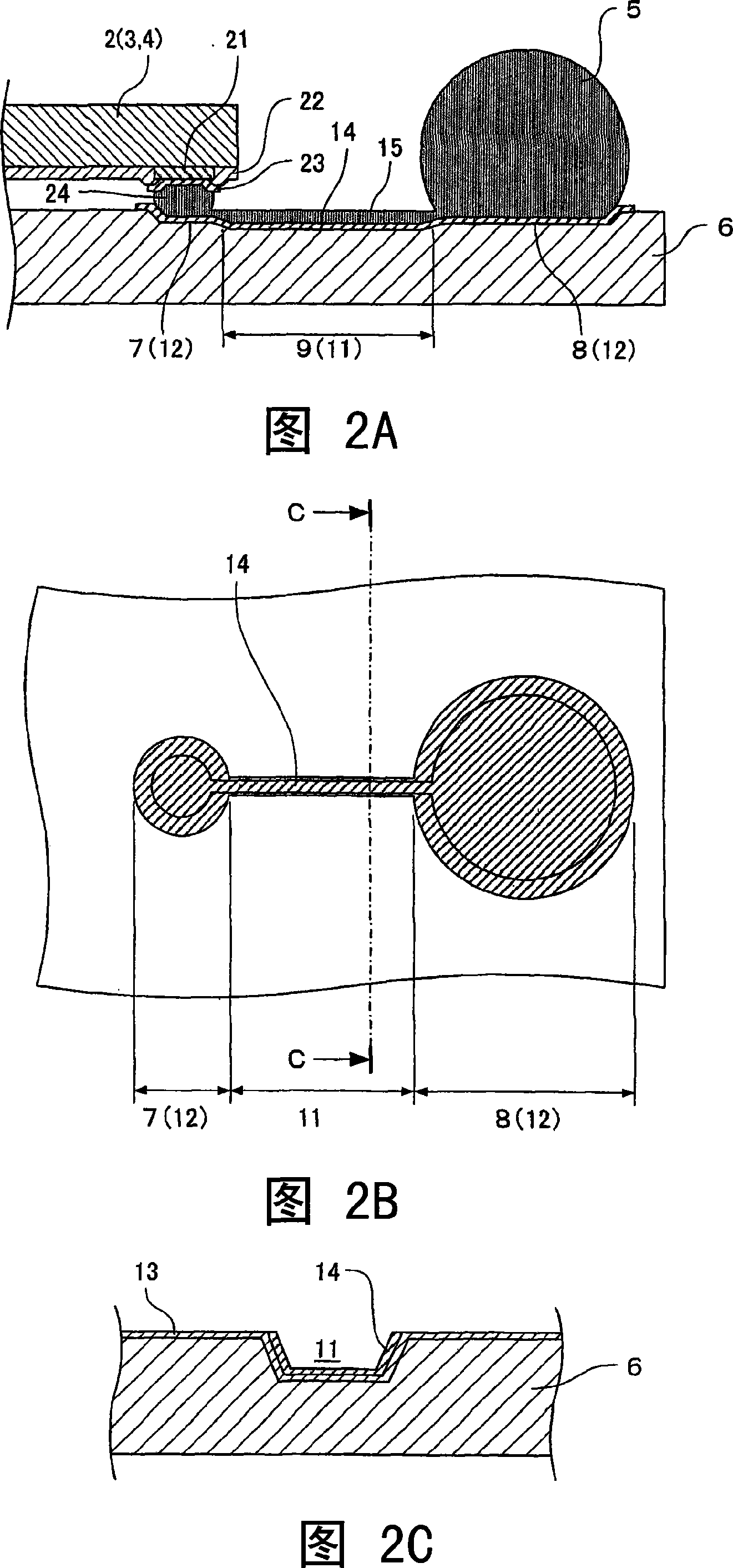
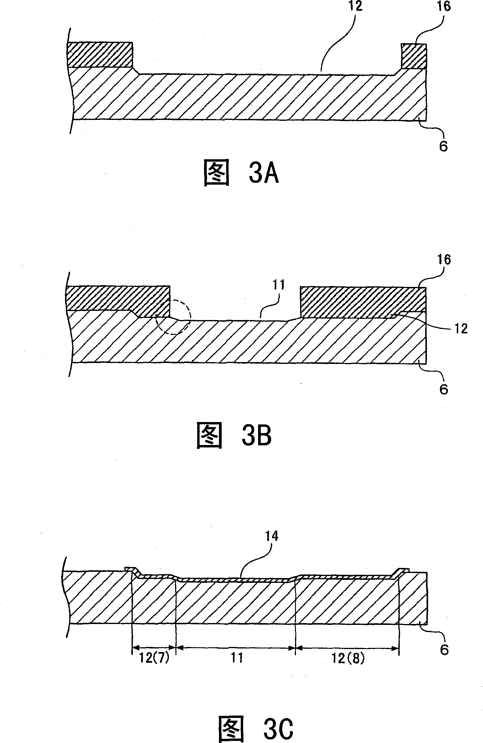
[0042] The structure of the wiring substrate 1 is that, on the surface of the silicon wiring substrate 6, there are a plurality of connection terminals 7 arranged in the central region, a plurality of external connection terminals 8 arranged in the peripheral region, and connections between the connection terminals 7 and the outside. The conductor wiring 9 to which the terminal 8 is connected. The plurality of connection terminals 7 are arranged in three predetermined areas on the wiring board 1, and the IC chips 2, 3, and 4 are mounted in the respective areas. The aforementioned solder balls 5 are formed on the external connection terminals 8 .

[0043] Here, the wiring board (hereinafter referred to as silicon wiring bo...


PUM


Abstract

A semiconductor device in accordance with the present invention includes IC chips (semiconductor elements) (2, 3, 4) having solder bumps (24) (projecting electrodes) formed on electrode pads, and a first wiring board (1) having connection terminals (7) to which the respective solder bumps (24) of the IC chips (2, 3, 4) are connected, external connection terminals (8) for connection to an external apparatus, and conductor wires (9) provided in respective groove portions formed in a board surface and connected to the respective connection terminals (7). In spite of the reduced pitch of the conductor wires (9), the presence of the groove portions enables an increase in cross section, allowing a reduction in wiring resistance.

Description

technical field [0001] The present invention relates to a semiconductor device and a manufacturing method thereof, and specifically relates to a semiconductor device composed of a semiconductor element (hereinafter referred to simply as an IC chip) forming a bump electrode (hereinafter referred to as an IC chip) and a wiring substrate and a manufacturing method thereof. Background technique [0002] As the functions of semiconductor devices increase and the processing speed increases, the number of electrode solder joints of IC chips connected to external circuits (hereinafter referred to as IC solder joints) also increases, and IC solder joints are formed around IC solder joints through leads and external circuits. There are limits to how wire bonds can be connected. Therefore, in order to make the size of the IC chip as small as possible and increase the number of IC solder joints at the same time, the flip-chip method is adopted to connect with external circuits through b...

Claims


Application Information

Patent Timeline
Patent Type & Authority Applications(China)
IPC IPC(8): H01L23/488H01L21/60
CPCH01L2924/19107H01L2924/04941H01L2224/16145H01L2924/00014H01L23/5386H01L2224/32225H01L2224/81801H01L2924/0105H01L2224/16225H01L2224/45124H01L23/49816H01L2924/01078H01L2924/01006H01L2924/01072H01L2224/81815H01L2224/49171H01L24/16H01L2924/01079H01L2924/15192H01L2924/01074H01L2924/14H01L25/0655H01L2924/15311H01L2224/16H01L2924/10253H01L2924/01024H01L2924/01005H01L2924/01082H01L2224/13099H01L2924/01013H01L2224/48465H01L2924/01022H01L2224/48227H01L2924/014H01L2924/01029H01L2224/8121H01L2924/01018H01L23/13H01L2924/157H01L2924/1532H01L24/81H01L2224/73265H01L2924/01033H01L2224/26175H01L2224/10175H01L2924/351H01L2224/05022H01L2224/05001H01L2224/05572H01L2224/05124H01L2224/056H01L24/05H01L2924/00
Inventor 青仓勇福田敏行太田行俊三木启司
Owner PANASONIC CORP
Why Eureka
Try Eureka