Method for manufacturing isolation structure

A manufacturing method and isolation structure technology, applied in semiconductor/solid-state device manufacturing, electrical components, circuits, etc., can solve problems such as increasing manufacturing costs and increasing process complexity

Inactive Publication Date: 2008-02-06
POWERCHIP SEMICON CORP
View PDF0 Cites 7 Cited by
  • Summary
  • Abstract
  • Description
  • Claims
  • Application Information

AI Technical Summary

Problems solved by technology

[0007] It can be seen from the above that when manufacturing two sets of shallow trench isolation structures with different depths, at least two photolithography and etching processes are required, which will increase the complexity of the process and increase the manufacturing cost.

Method used


Image

  • Method for manufacturing isolation structure
  • Method for manufacturing isolation structure
  • Method for manufacturing isolation structure

Examples


Embodiment Construction

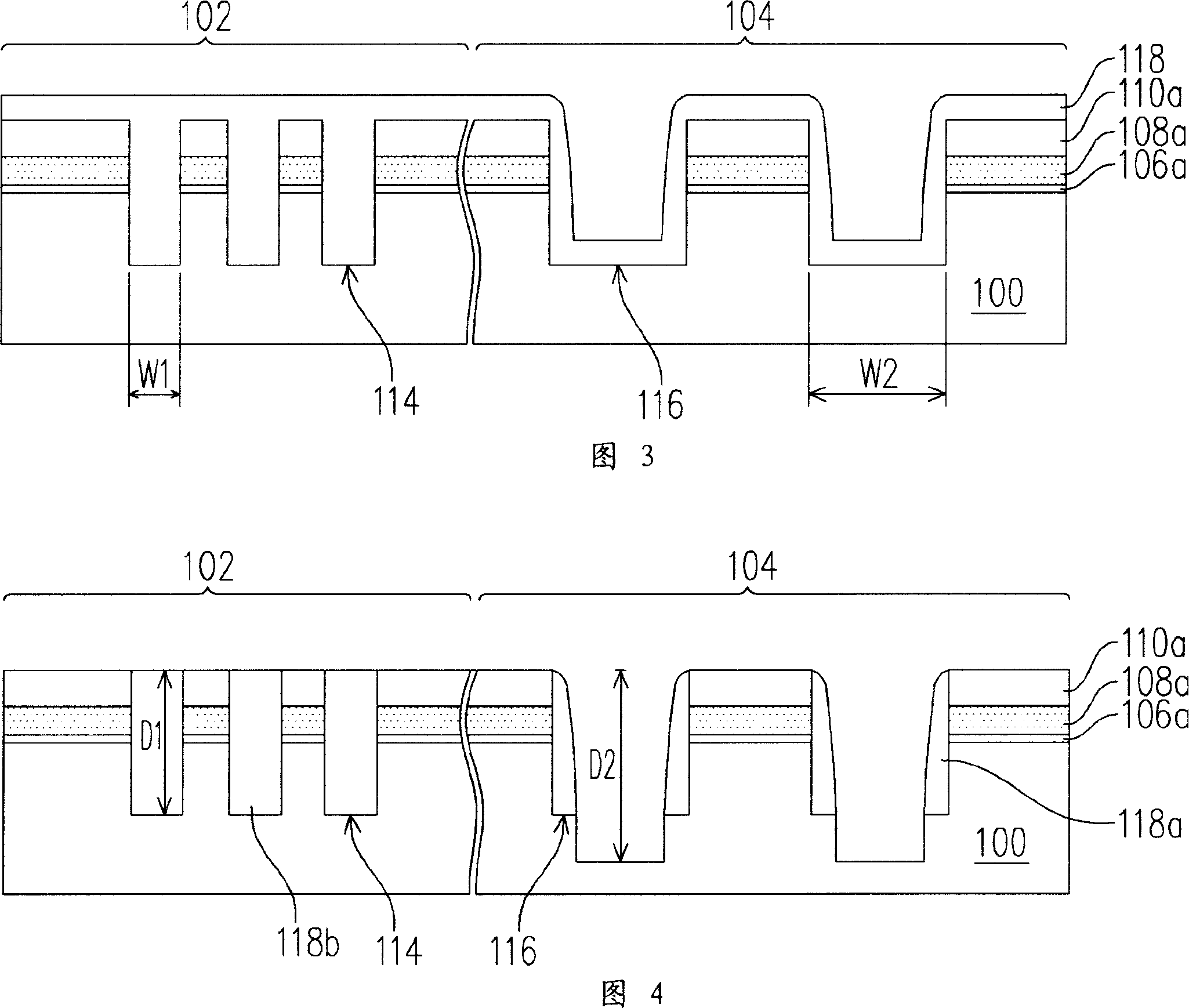
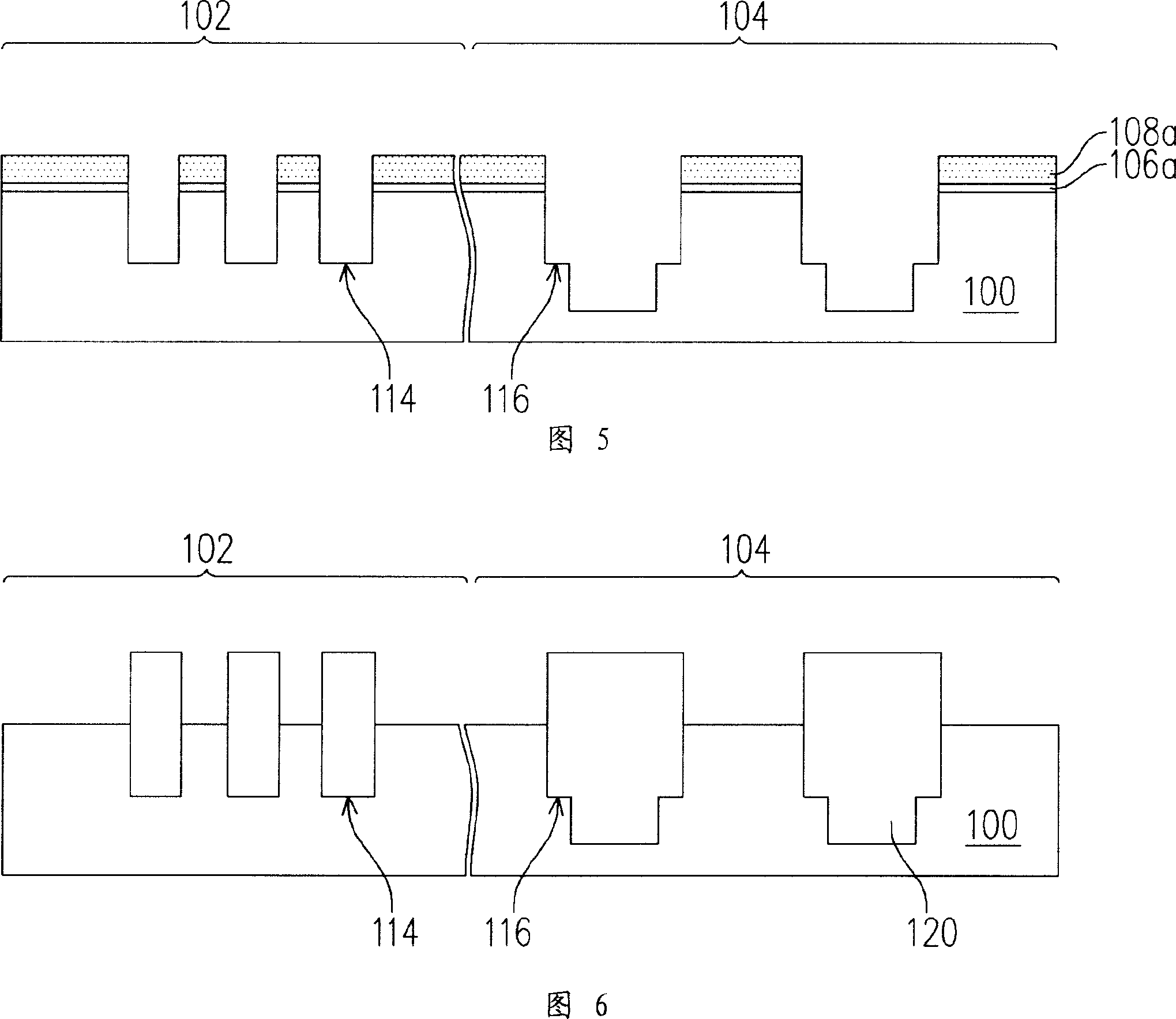
[0035] In view of the shortcomings of the prior art, the present invention provides a method for manufacturing an isolation structure. In this manufacturing method, two groups of grooves with different widths are firstly formed on the substrate. Afterwards, a spacer is formed on the sidewall of the wider trench, and at the same time, the material of the spacer fills up the narrower trench. Then, using the self-aligned principle, the part of the substrate exposed by the spacer is removed by using the spacer as a mask, so as to deepen the depth of the trench. Afterwards, a dielectric layer is formed in the two groups of trenches to form an isolation structure.

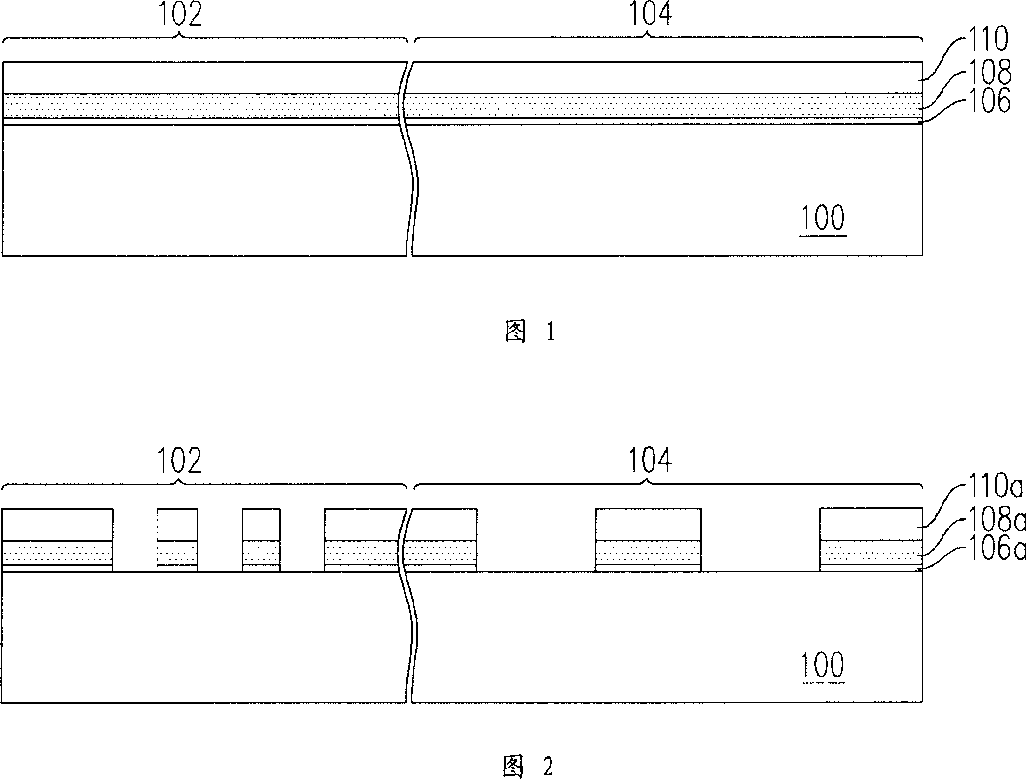
[0036] 1 to 6 are cross-sectional flowcharts of a method for manufacturing an isolation structure according to an embodiment of the present invention.

[0037] Referring to FIG. 1 , firstly, a substrate 100 is provided. The substrate 100 is, for example, a silicon substrate. The substrate 100 can be divided into a fi...


PUM


Abstract

The present invention relates to a manufacturing method for the separation structure. Firstly, a substrate is provided and the substrate is patternized, in the substrate, a first groove and a second groove are formed, wherein the width of the first groove is less than that of the second groove. Secondly, a common shaped insulation layer is formed on the substrate. Thirdly, a part of insulation layer is removed to facilitate the rest of insulation layer to fill up the first groove and form a plurality of spacing walls on the side walls of the second groove. A part of the substrate on the bottom of the second groove between the spacing walls is removed to ensure that the depth of the second groove is larger than that of the first groove. Lastly, inside the first groove and the second groove, a dielectric layer is formed.

Description

technical field [0001] The invention relates to a semiconductor process, in particular to a method for manufacturing an isolation structure with two depths. Background technique [0002] As the integration of internal units of integrated circuit chips continues to increase, the possibility of unnecessary electronic interference between adjacent units will increase. For example, complementary metal oxide semiconductor (CMOS) is prone to latch-up, and the latch-up will be more severe in highly integrated integrated circuits. Therefore, an integrated circuit must have a proper isolation structure to avoid unit-to-unit interference. [0003] Among various isolation structures, an isolation structure (local oxidation of silicon, LOCOS) formed by a local oxidation method has been widely used in various integrated circuits. However, because the area oxidation method will reduce the area of ​​the active area (active area), reduce the performance of the unit, and increase the diffi...

Claims


Application Information

Patent Timeline
Patent Type & Authority Applications(China)
IPC IPC(8): H01L21/762
Inventor 魏鸿基毕嘉慧
Owner POWERCHIP SEMICON CORP
Why Eureka
Try Eureka