Light-emitting device and illuminating device

A technology for light-emitting devices and light-emitting elements, which is applied to electrical components, electric solid-state devices, circuits, etc., can solve the problems of low on-axis luminosity, large emission angle, increased light loss, etc., and achieves improved emission light intensity and light extraction efficiency. High, the effect of suppressing color variation

Inactive Publication Date: 2008-02-13
KYOCERA CORP
View PDF1 Cites 24 Cited by
  • Summary
  • Abstract
  • Description
  • Claims
  • Application Information

AI Technical Summary

Problems solved by technology

[0009] However, in the case of the conventional light-emitting device 211, there are the following problems: that is, the light emitted to the lower side of the phosphor layer 217 after wavelength conversion by the phosphor layer 217, and the light emitted from the upper side of the phosphor layer 217 after emitting light from the light-emitting element. The light emitted from the surface to the lower side is repeatedly reflected and attenuated inside the case 213, and is absorbed by the substrate 212 or the light emitting element 214, resulting in a significant increase in light loss
[0010] In addition, there is the following problem: that is, the light emitted obliquely upward from the light emitting element 214 is not reflected by the casing 213, but outside the light emitting device 211 Emitted at a larger launch angle, so the launch angle is larger and the on-axis luminosity is lower

Method used


Image

  • Light-emitting device and illuminating device
  • Light-emitting device and illuminating device
  • Light-emitting device and illuminating device

Examples


no. 1 Embodiment approach

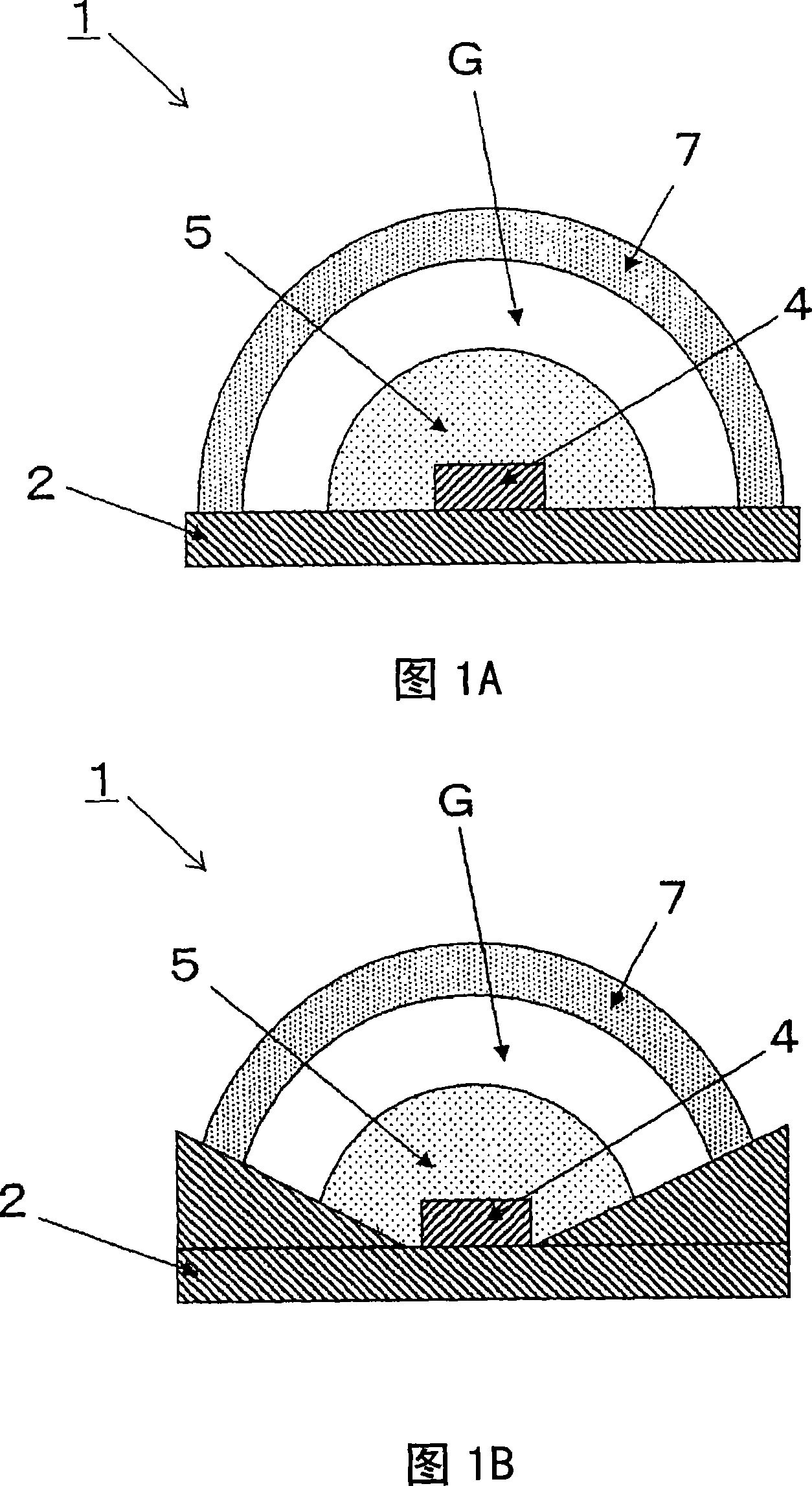
[0069] 1A and 1B are cross-sectional views showing the first embodiment of the present invention. First, as shown in FIG. 1A, the light-emitting device 1 is composed of a base 2, a light-emitting element 4, a first light-transmitting portion 5, a second light-transmitting portion 7, a third light-transmitting portion G, and the like.

[0070] On the base 2, a wiring conductor for supplying current to the light-emitting element 4 is formed extending from the upper surface to the lower surface or the side surface.

[0071] The light emitting element 4 is mounted on the upper surface of the base 2 so as to be electrically connected to the wiring conductor of the base 2.

[0072] The first light-transmitting portion 5 is formed of a light-transmitting material, and covers the light-emitting element 4.

[0073] The second translucent portion 7 is formed of a translucent material containing a phosphor that converts the wavelength of light emitted by the light-emitting element 4, and is ...

no. 2 Embodiment approach

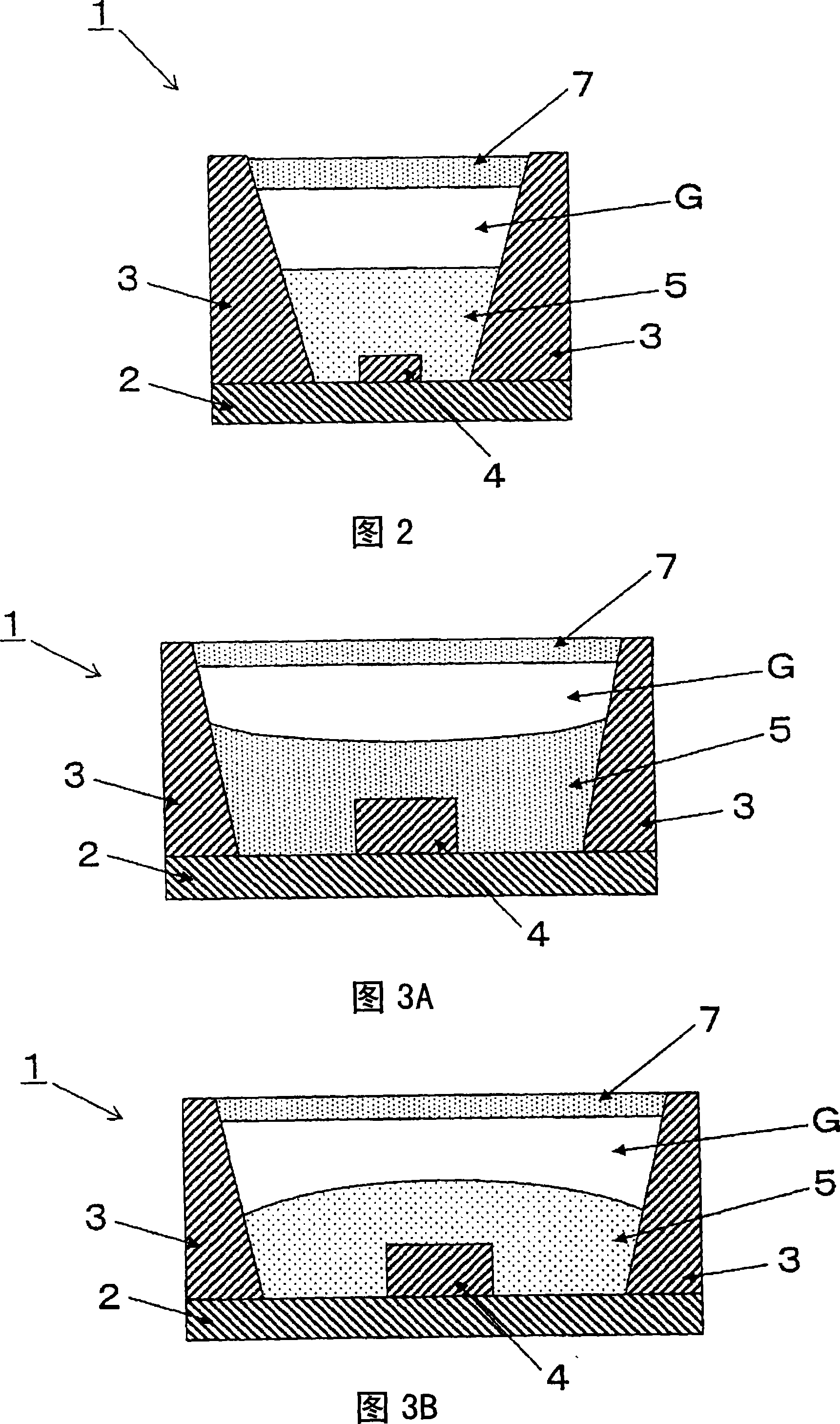
[0089]Fig. 2 is a cross-sectional view showing a second embodiment of the present invention. The light-emitting device 1 is composed of a base 2, a housing 3, a light-emitting element 4, a first light-transmitting portion 5, a second light-transmitting portion 7, a third light-transmitting portion G, and the like.

[0090] On the base 2, a wiring conductor for supplying current to the light emitting element 4 is arranged from the upper surface to the lower surface or to the side surface.

[0091] The light emitting element 4 is mounted on the upper surface of the base 2 so as to be electrically connected to the wiring conductor of the base 2.

[0092] The casing 3 is fixed on the base 2 and has an inner surface inclined upward in a manner of surrounding the light emitting element 4. It is preferable that the inner surface of the housing 3 has light reflectivity from the viewpoint of light use efficiency.

[0093] The first light-transmitting portion 5 is formed of a light-transmit...

no. 3 Embodiment approach

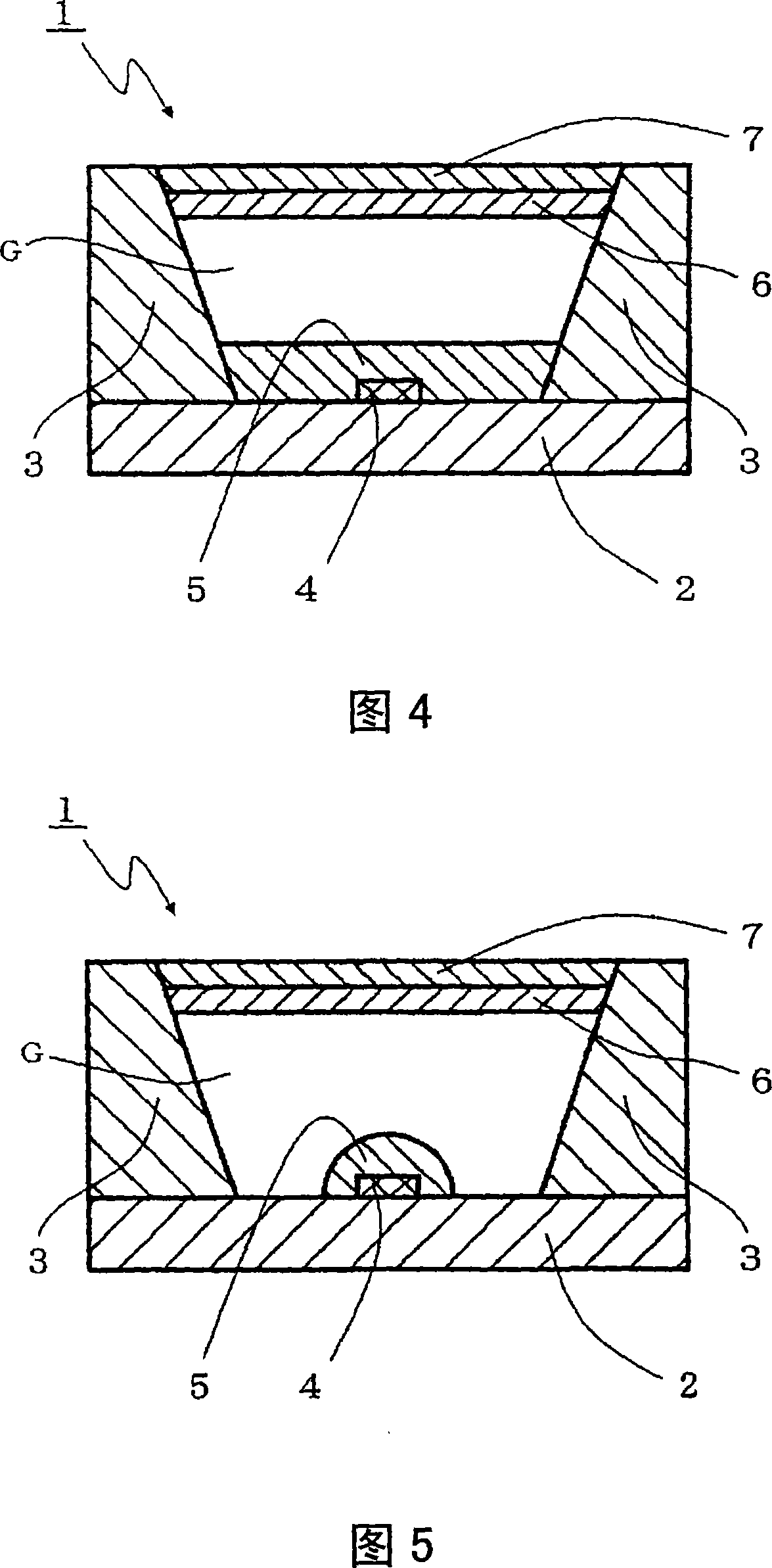
[0106] 3A and 3B are cross-sectional views showing a third embodiment of the present invention. First, as shown in FIG. 3A, the light-emitting device 1 is composed of a base 2, a housing 3, a light-emitting element 4, a first light-transmitting portion 5, a second light-transmitting portion 7, a third light-transmitting portion G, and the like.

[0107] On the base 2, a wiring conductor for supplying current to the light emitting element is formed extending from the upper surface to the lower surface.

[0108] The light emitting element 4 is mounted on the upper surface of the base 2 so as to be electrically connected to the wiring conductor of the base 2.

[0109] The housing 3 is fixed on the base 2 and has an inner surface inclined upward so as to surround the light emitting element 4. It is preferable that the inner surface of the housing 3 has light reflectivity from the viewpoint of light use efficiency.

[0110] The first light-transmitting portion 5 is formed of a light-tr...


PUM


Abstract

A light-emitting device comprises a base where a wiring conductor is formed over the top to bottom surfaces or over the top to side surfaces, a light-emitting element mounted on the top surface of the base and electrically connected to the wiring conductor, a first light-transmitting section covering the light-emitting element, a second light-transmitting section disposed over the first light-transmitting section, covering the first light-transmitting element, and made of a light-transmitting material containing a phosphor for converting the wavelength of the light emitted from the light-emitting element and a third light-transmitting section interposed between the first and second light-transmitting sections. The following relations are satisfied: n3 H01L 33/00 9 29 2 2005/7/27 101124683 2008/2/13 000000000 Kyocera Corp. Japan Tabuchi Tomoya Miyake Akira Sakumoto Daisuke lixiang lan 11021 The Patent Agency of the Chinese Academy of Sciences Inside the Chinese Academy of Sciences, No.52 Sanlihe Road, Fuwai, Beijing 100864 Japan 2004/12/24 375037/2004 Japan 2005/1/24 016054/2005 2007/8/17 PCT/JP2005/013749 2005/7/27 WO2006/067885 2006/6/29 Japanese

Description

Technical field [0001] The present invention relates to a light-emitting device that converts light emitted by a light-emitting element using phosphors and emits it to the outside, and a lighting device using the same. Background technique [0002] FIG. 18 shows a conventional light-emitting device 211 for housing a light-emitting element 214 such as a light-emitting diode (LED). As shown in FIG. 18, the light-emitting device has a mounting portion 212a on which the light-emitting element 214 is mounted at the center of the upper surface, and is mainly composed of the following devices: a base 212 formed with wiring conductors (not shown) The wiring conductor is composed of lead terminals or metalized wiring that electrically connect the mounting portion 212a and its periphery to the inside and outside of the light-emitting device; and the housing 213, which is adhesively fixed to the base On the upper surface of 212, a through hole for accommodating the light-emitting element 21...

Claims


Application Information

Patent Timeline
Patent Type & Authority Applications(China)
IPC IPC(8): H01L33/00H01L33/60H01L33/62
CPCH01L2224/16225H01L2924/181
Inventor 田渊智也三宅彻作本大辅
Owner KYOCERA CORP
Why Eureka
Try Eureka