

Semiconductor device and wire bonding method used for the same
A semiconductor and wire connection technology, applied in the direction of semiconductor devices, semiconductor/solid-state device manufacturing, semiconductor/solid-state device components, etc., which can solve problems such as increasing bond pads and contact dimensions
- Summary
- Abstract
- Description
- Claims
- Application Information
AI Technical Summary
Problems solved by technology
Method used
Image

Examples
no. 1 approach
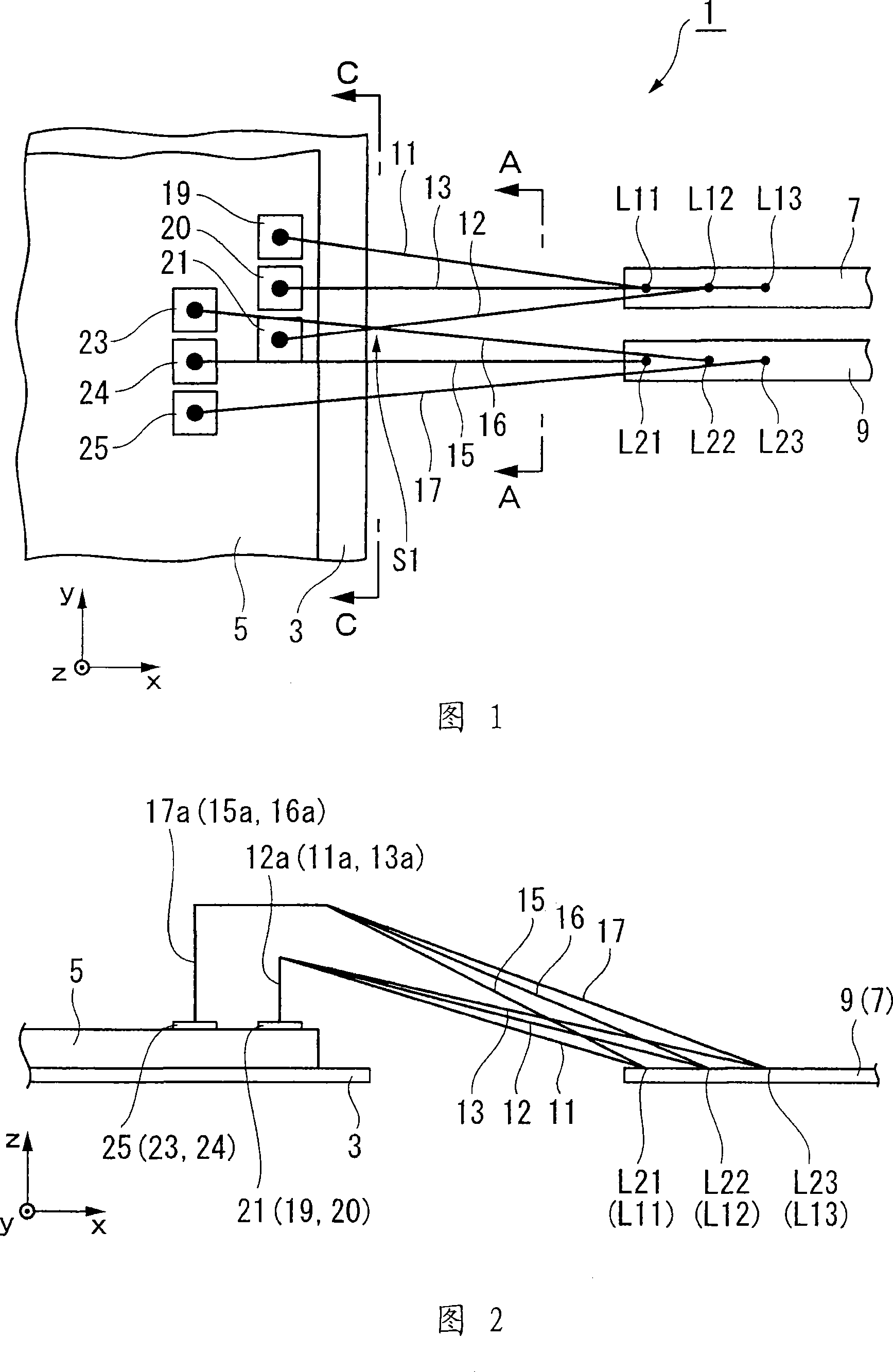
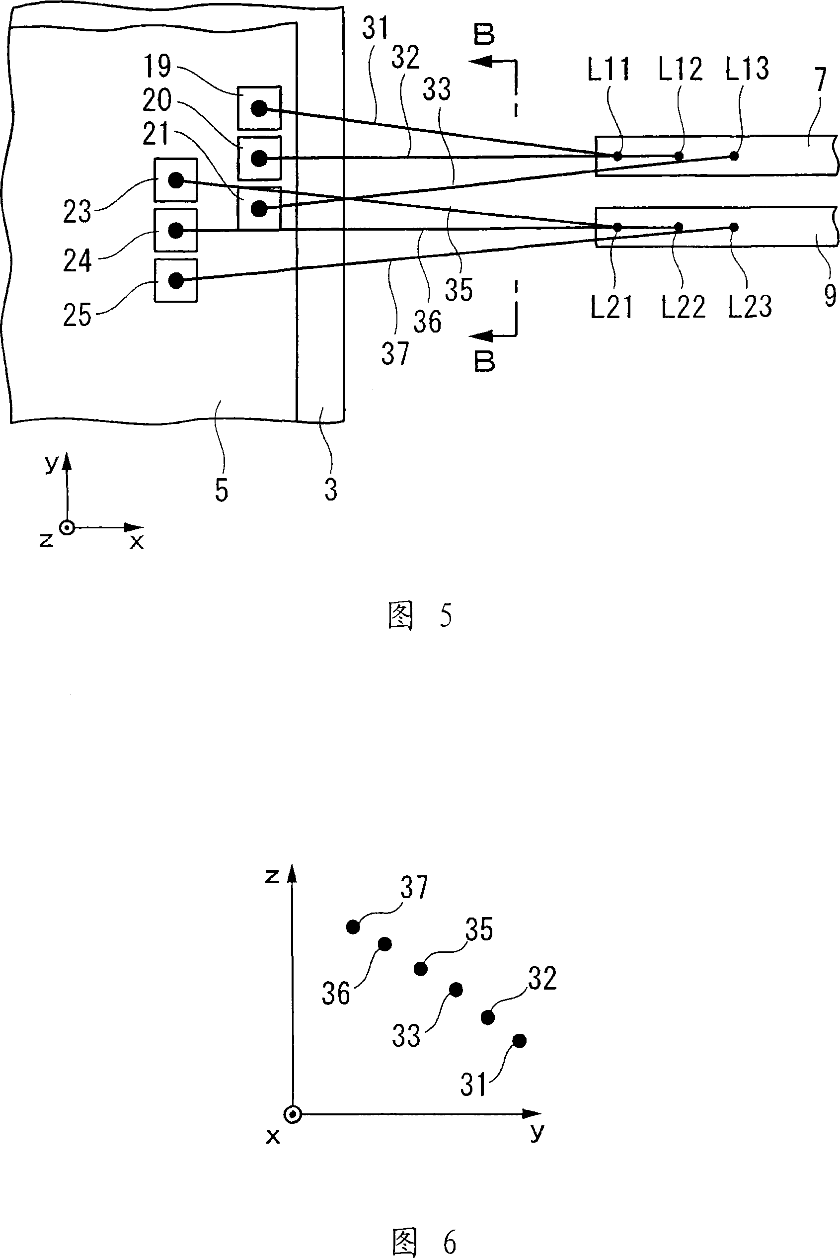
[0068] A semiconductor device 1 according to a first embodiment of the present invention will be described with reference to FIGS. 1 to 4 . As shown in FIGS. 1 and 2, a plurality of pins 7 and 9 arranged adjacent to each other are arranged on the periphery of a semiconductor chip 5 mounted on a stage 3 having a planar shape, wherein the pin 7 is electrically connected via three leads 15 to 17. to three electrode pads 19 to 21, and the pin 9 is electrically connected to three electrode pads 23 to 25 via three lead wires 15 to 17. A plurality of sets of pins connected via three leads and three electrodes are arranged for the semiconductor chip 5 .
[0069] Each pin 7 and 9 has an elongated shape extending toward the semiconductor chip 5 . The second bonding objects L11 to L13 connected to the leads 11 to 13 are arranged longitudinally along the lead wire 7 , and the second bonding objects L21 to L23 connected to the leads 15 to 17 are arranged longitudinally along the lead wire...
no. 2 approach
[0102] Next, a wire bonding method according to a second embodiment of the present invention will be described with reference to FIGS. 7A to 7C , FIGS. 8A and 8B , FIGS. 9A to 9C , FIGS. 10A and 10B , and FIGS. 11A and 11B . As shown in FIGS. 7A-7C, 8A, 8B, 9A, and 9B, a wire bonding method is performed so that bonding pads 101a formed on a semiconductor chip 101 mounted on a board 103 and bonding pads 101a formed on the board 103 are connected via metal wires 105. Electrical connections are established between electrode pads (or connection pads) 103a around the semiconductor chip 101 .
[0103] As shown in FIG. 7A , the semiconductor chip 101 is pre-mounted on the board 103 such that electrode pads 103 a are formed on the board 103 at the periphery of the semiconductor chip 101 . Here, the small-diameter capillary 109 is used to provide the thin lead wire 107 whose diameter is smaller than that of the metal wire 105 . The tip of the small-diameter capillary 109 is pressed on...
no. 3 approach
[0131] A semiconductor device 201 according to a third embodiment of the present invention will be described with reference to FIGS. 12 to 14 . As shown in FIGS. 12 and 13 , a semiconductor chip 205 is mounted on a surface 203a of a stage 203 having a planar shape in plan view, with a plurality of electrode pads 207 and 209 formed on the surface 205a of the semiconductor chip 205 . A plurality of pins 211 and 213 line the periphery of the semiconductor chip 205 in which they are connected to electrode pads 207 to 209 via a plurality of leads 215 to 217 .
[0132]In the semiconductor chip 201, the stage 203, the semiconductor chip 205, and the leads 215 and 217 are sealed with the mold resin 219, and the mold resin 219 also integrally fixes the stage 203, the semiconductor chip 205, the pins 211 and 213, and the leads 215 and 217. at the intended location.
[0133] The electrode pads 207 and 209 are alternately arranged along different lines on the surface 205 a of the semicon...
PUM
 Abstract
Description
Claims
Application Information