Embedded waveguide printed circuit board structure

A printed circuit board, embedded technology, applied in the direction of printed circuit, printed circuit, printed circuit manufacturing, etc., can solve the problem that the waveguide is not easy to integrate, and achieve the effect of reducing the change of dielectric loss and crosstalk

Inactive Publication Date: 2008-02-20
INTEL CORP
View PDF0 Cites 7 Cited by
  • Summary
  • Abstract
  • Description
  • Claims
  • Application Information

AI Technical Summary

Problems solved by technology

Standard waveguides are not easily integrated into digital systems based on current printed circuit board (PCB) process technology

Method used


Image

  • Embedded waveguide printed circuit board structure
  • Embedded waveguide printed circuit board structure
  • Embedded waveguide printed circuit board structure

Examples


Embodiment Construction

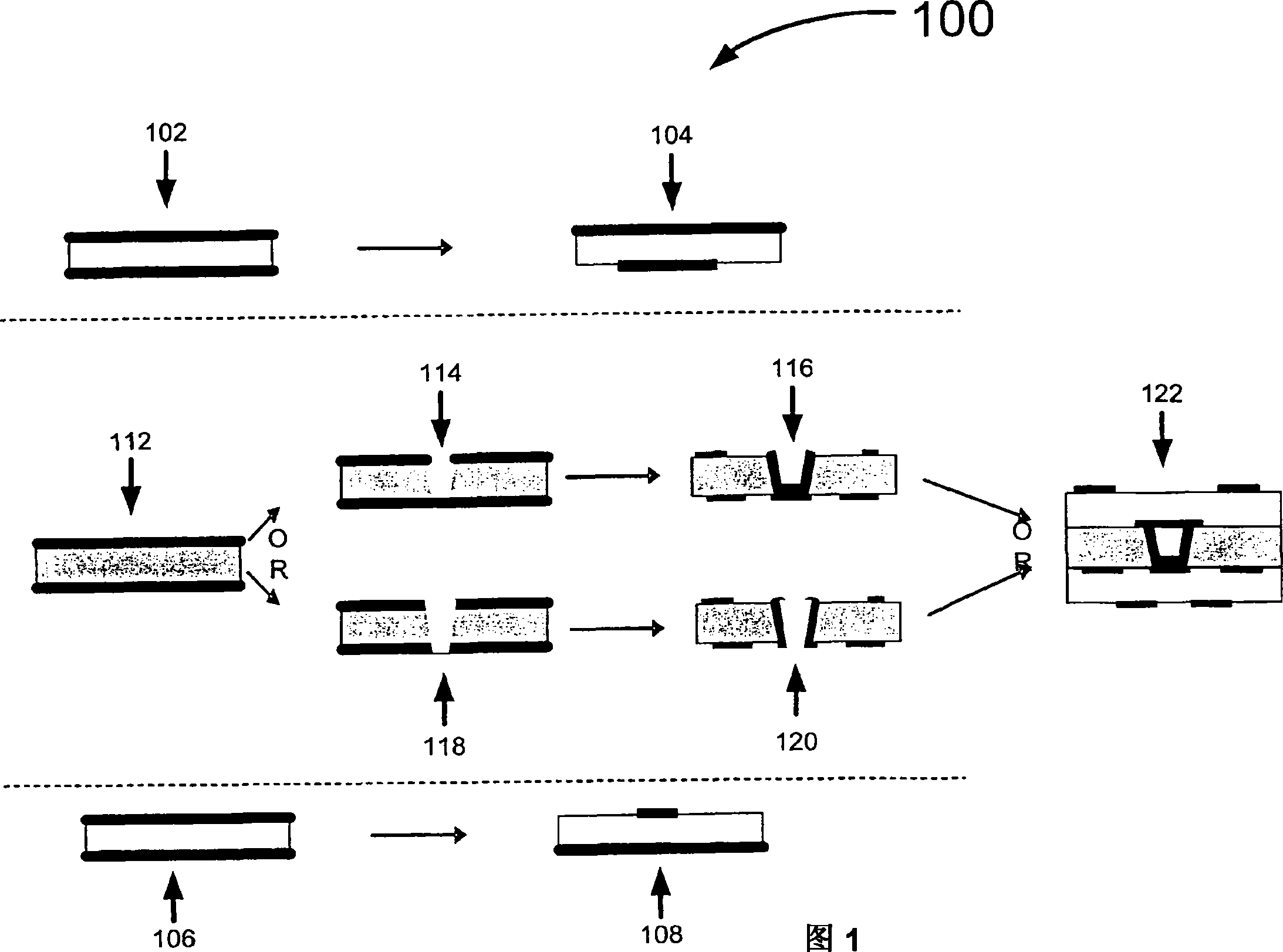
[0042] FIG. 1 illustrates a process 100 of forming waveguides in accordance with some embodiments. According to some embodiments, process 100 uses a thermoplastic cap material of thermoplastic nature to attach the top cap and / or bottom cap of the waveguide during lamination.

[0043] The top portion of the process 100 of FIG. 1 shows at 102 a copper clad thermoplastic dielectric core or multilayer structure. According to some embodiments, a copper clad thermoplastic dielectric core or multilayer structure shown at 102 has a bottom dielectric composed of thermoplastic. The bottom copper layer is imaged at 104 . The bottom copper layer, shown at 104, includes the conductors used to form the air dielectric waveguide.

[0044] Similar to the top portion of the process 100 of FIG. 1 , the bottom portion of the process 100 includes at 106 a copper clad thermoplastic dielectric core or a multilayer structure with the top dielectric being thermoplastic. The top copper layer of the ...


PUM


Abstract

In some embodiments a channel is formed in printed circuit board material, the formed channel is plated to form at least two side walls of an embedded waveguide, and printed circuit board material is laminated to the plated channel. Other embodiments are described and claimed.

Description

[0001] related application [0002] This application is related to the US patent with the application serial number "Pending", the title of the invention "Printed Circuit Board Waveguide (Printed Circuit Board Waveguide)", and the attorney case number 042390.P23385, which was filed on the same day and has the same inventor as this application. [0003] This application is related to the application serial number "Pending" filed on the same day and having the same inventor as this application, the title of the invention is "Imprinted Waveguide Printed Circuit Board Structure (Imprinted Waveguide Printed Circuit Board Structure)", and the attorney case number is 042390. US Patent P21427. [0004] This application is also related to the application serial number "pending" filed on the same day and having the same inventor as this application, the title of the invention is "Quasi-Waveguide Printed Circuit Board Structure (Quasi-Waveguide Printed Circuit Board Structure)", and the a...

Claims


Application Information

Patent Timeline
IPC IPC(8): H05K3/00H05K3/46H05K1/02
CPCH05K2201/09981H05K1/024H05K2201/037H05K3/4614H01P3/121H05K1/0272H05K3/4611H01P11/002H05K2201/0379H05K3/462
Inventor G·A·布里斯特B·D·霍赖恩S·哈尔
Owner INTEL CORP
Why Eureka
Try Eureka