Method for forming microlens array structure

A technology of microlens array and surface shape, which is applied to the photoplate process of lens and pattern surface, optics, etc., can solve the problems of complex process, low production efficiency, high cost, etc., and achieve simple production process and reduced data volume Effect

Inactive Publication Date: 2008-03-19
四川中科铭源光电科技有限公司
View PDF0 Cites 16 Cited by
  • Summary
  • Abstract
  • Description
  • Claims
  • Application Information

AI Technical Summary

Problems solved by technology

At present, a variety of methods have been developed that can be used to make micro-lens arrays, such as photolithography hot-melt method, laser direct writing method, gray scale mask method, etc. The surface finish of micro-optical elements formed by photolithography hot-melt method is high, but only Forming components with a hemispherical surface; laser direct writing can form any surface structure, but the production efficiency is lo

Method used


Image

  • Method for forming microlens array structure
  • Method for forming microlens array structure
  • Method for forming microlens array structure

Examples


Embodiment Construction

[0031] The present invention will be described in detail below in conjunction with specific embodiments and accompanying drawings, but the scope of protection of the present invention is not limited to the following examples, and should include all content in the claims.

[0032] The process of the method forming microlens array structure of the present invention is as follows:

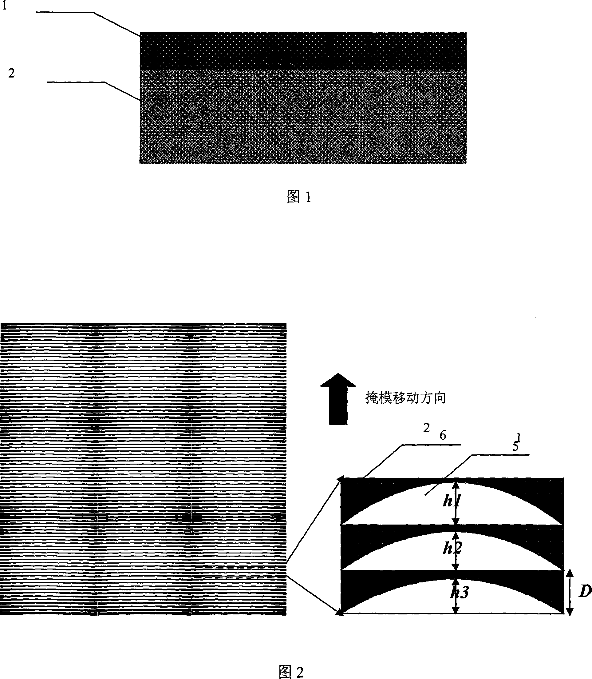
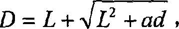
[0033] (1) Choose germanium Ge material as the substrate, and coat the photoresist AZ9260 on its surface, the speed of the glue-spinning machine is 5000 rpm / s, the glue-spinning time is 30s, the pre-baking temperature is 65°C, and the pre-baking time is 25min, As shown in Figure 1;

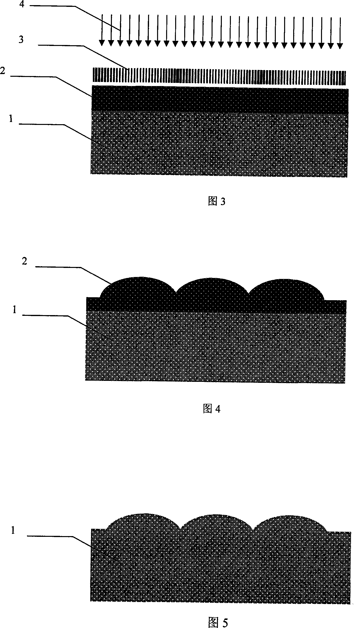
[0034] (2) For a lens with an aperture of 1.5 mm, an ISI 1802 laser direct writing system is used to make a mask, and the system parameters are: d=0.1 μm, L=1 μm. Use the aforementioned formula (1) to calculate and determine the optimal sampling interval, and obtain D=13.28 μm. In order to make the sampling number an int...


PUM


Abstract

A method to shape an array structure of a microlens involves the steps as follow: (1) a substrate is chosen to be coated with a resist layer on the surface; (2) the substrate coated with resist layer is pre-baked; (3 ) three-dimensional array target surfaces are sampled to design a mask; (4)the mask designed before can be used to expose; (5) the substrate after being exposed is developed and post-baked; (6) surface shapes can be transferred to the substrate by RIE reactive Ion etching art. With simple processing art and high efficiency, the present invention can shape microlens array in various surface shapes and calibers.

Description

technical field [0001] The invention belongs to the technical field of micro-nano structure processing, in particular to a method for forming a micro-lens array structure. Background technique [0002] Due to its light weight, small size, and flexible design, microlens arrays have played more and more roles in optical fiber communication, Shack-Hatrmann sensing, aerospace, biomedicine, and laser-machining. At present, a variety of methods have been developed that can be used to make micro-lens arrays, such as photolithography hot-melt method, laser direct writing method, gray scale mask method, etc. The surface finish of micro-optical elements formed by photolithography hot-melt method is high, but only Forming components with a hemispherical surface; laser direct writing can form any surface structure, but the production efficiency is low and the cost is high. It is only used for the production of masks, not directly for forming microlens arrays; grayscale masks Although t...

Claims


Application Information

Patent Timeline
IPC IPC(8): G03F7/00G02B3/00
Inventor 杜春雷董小春史立芳邓启凌
Owner 四川中科铭源光电科技有限公司
Why Eureka
Try Eureka