Driving circuit and driving method of liquid crystal device, liquid crystal device, and electronic apparatus

A technology of liquid crystal device and driving circuit, which is applied in the field of improving display quality and liquid crystal device

Inactive Publication Date: 2008-04-02
EPSON IMAGING DEVICES CORP
View PDF1 Cites 11 Cited by
  • Summary
  • Abstract
  • Description
  • Claims
  • Application Information

AI Technical Summary

Problems solved by technology

Therefore, it is difficult to apply the above-mentioned background technology to so-called IPS (In-Plane Switching) and FFS (Fringe Field Switching) liquid crystal...

Method used


Image

  • Driving circuit and driving method of liquid crystal device, liquid crystal device, and electronic apparatus
  • Driving circuit and driving method of liquid crystal device, liquid crystal device, and electronic apparatus
  • Driving circuit and driving method of liquid crystal device, liquid crystal device, and electronic apparatus

Examples


no. 1 Embodiment

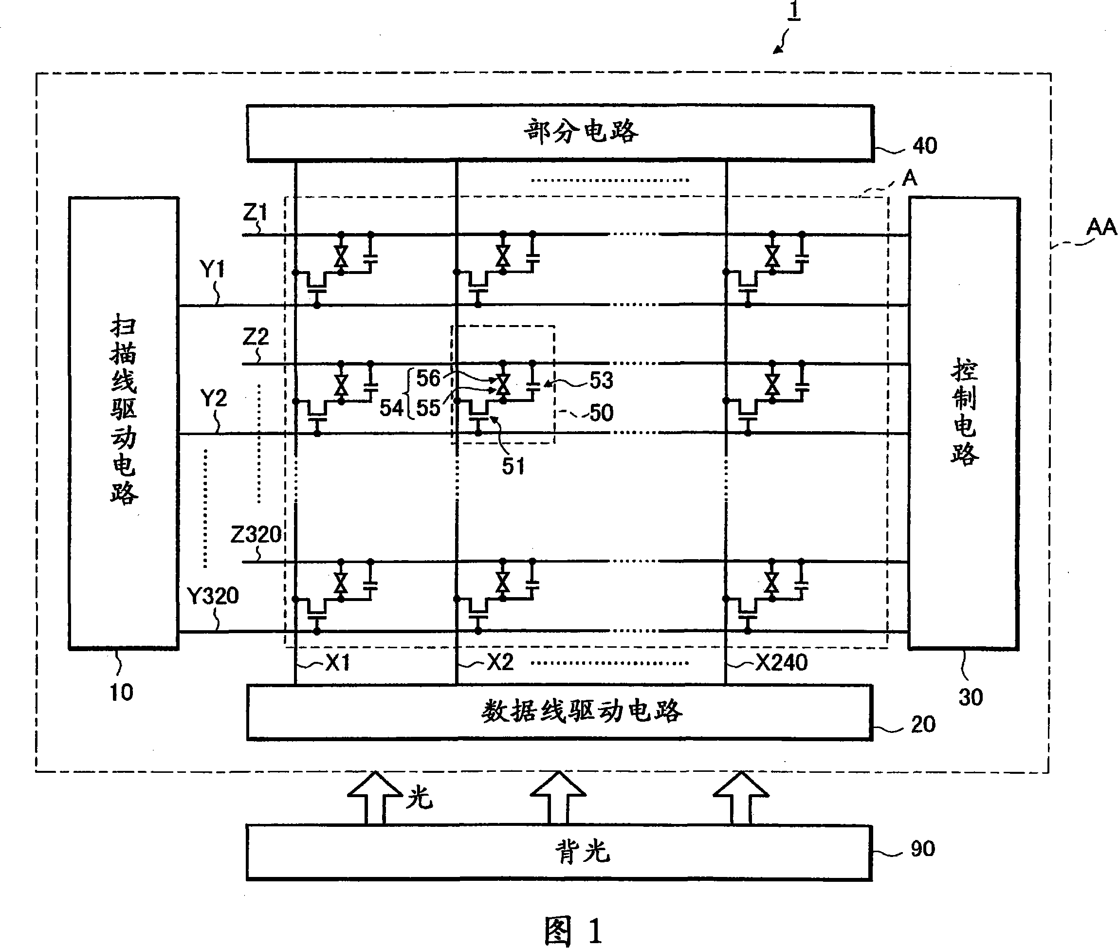
[0097] First, a liquid crystal device related to a first embodiment of the present invention will be described. FIG. 1 is a block diagram showing the configuration of a liquid crystal device 1 related to the first embodiment.

[0098] As shown in the figure, the liquid crystal device 1 includes a liquid crystal panel AA and a backlight 90 that emits light and is disposed on the opposite side of the liquid crystal panel AA. This liquid crystal device 1 performs transmissive display using light emitted from the backlight 90 .

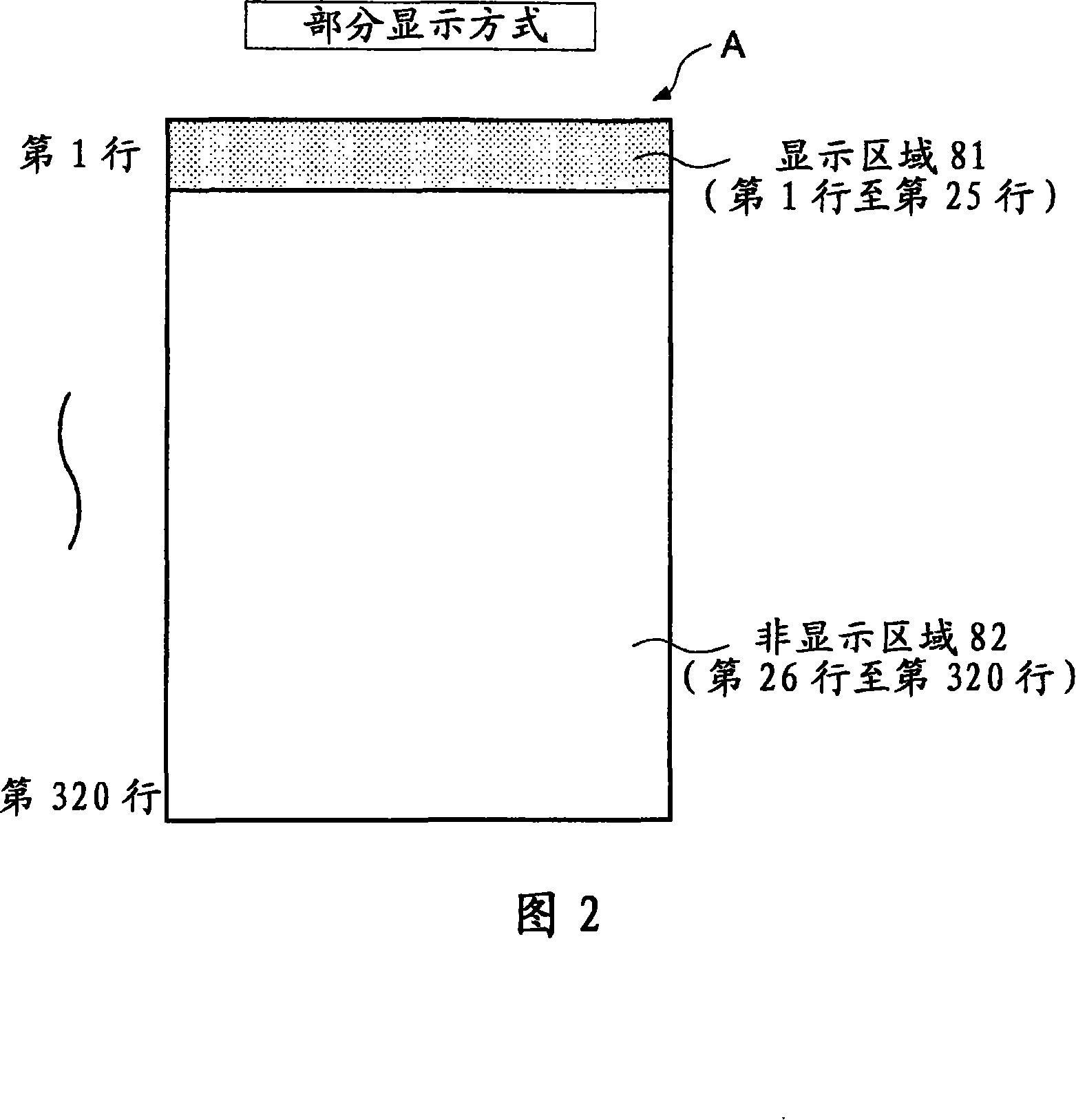
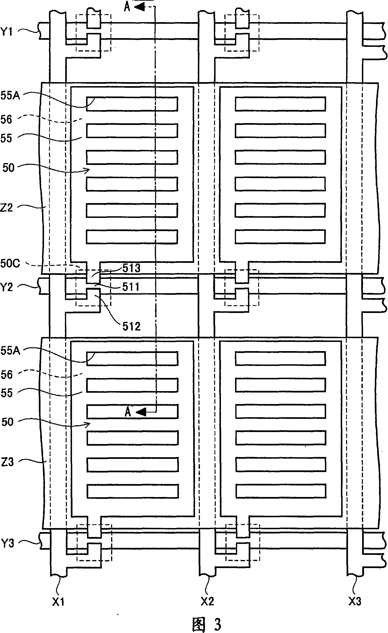
[0099] The liquid crystal panel AA has a display screen A, a scanning line driving circuit 10 , a data line driving circuit 20 , a control circuit 30 and some circuits 40 . Wherein, on the display screen A, a plurality of pixels 50 are arranged in a matrix to display images. The scanning line driving circuit 10 and the data line driving circuit 20 are arranged around the display screen A and function as a driving circuit for driving the display panel AA...

no. 2 Embodiment

[0339] Next, a liquid crystal device related to a second embodiment of the present invention will be described.

[0340] In the liquid crystal device related to the second embodiment, the circuit configuration of the control circuit 30 (see FIG. 6) in the first embodiment is changed, and FIG. 21 is a block diagram showing the configuration of the modified control circuit 30A.

[0341] In addition, the partial circuit 40 in the second embodiment supplies the voltage VCENT as a predetermined voltage to the data lines X1-X240 when a selection voltage is applied to the scanning lines related to the non-display area 82 in the partial display mode. In addition, since other constructions are the same as those of the first embodiment, description thereof will be omitted.

[0342] As shown in the figure, the control circuit 30A has the same latch circuit 31 as that of the first embodiment, but has a display mode circuit 32A and a voltage selection circuit 33A having different circuit s...

no. 3 Embodiment

[0390] Next, a liquid crystal device related to a third embodiment of the present invention will be described.

[0391] In the liquid crystal device related to the third embodiment, the pixel 50 in the first embodiment is changed (see FIG. 3 ). FIG. 30 is an enlarged plan view showing the structure of a pixel 50A related to the third embodiment. In addition, the pixel 50A related to the third embodiment differs from the pixel 50 of the first embodiment in that it has an auxiliary common line ZA and a contact wiring 58 . Other structural aspects are the same as those of the first embodiment, so descriptions are omitted.

[0392] The auxiliary common line ZA is formed of a conductive metal film and is divided row by row, that is, it is formed along the scanning line Y so as to correspond to the common electrode 56 (common line). Specifically, the auxiliary common line ZA of a certain row is formed along the direction of the scanning line between the scanning line of the row an...


PUM


Abstract

The invention relates to a driving circuit, a liquid crystal device, an electronic device and a method for driving the liquid crystal device, which can restraining the decrease of the display quality at the same time of decreasing the power consumption. A pixel electrode and a common electrode which form a pixel capacitor are arranged on one of a pair of substrates used for holding the liquid crystal device. The liquid crystal device 1is provided with a scanning line driving circuit 10, a data line driving circuit 20, a control circuit 30 and partial circuits 40. In the display area under the full screen display mode and the partial screen display mode, the data line driving circuit 20 supplies the data line X with image signals after the control circuit 30 supplies a common electrode 56 with a voltage VCOML and a voltage VCOMH. In the non-display area under the partial screen display mode, if the control circuit 30 supplies the common electrode 56 with the voltage VCOML, the partial circuits 40 supply the data line X with voltage VCOMH.

Description

technical field [0001] The invention relates to a technique for improving display quality in a liquid crystal device in which a pixel electrode and a common electrode are arranged on a substrate. Background technique [0002] Liquid crystal devices that display images using liquid crystals have been known in the past. This liquid crystal device has, for example, a liquid crystal panel and a backlight arranged on the opposite side of the liquid crystal panel. Among them, the liquid crystal panel is composed of a pair of substrates and liquid crystal sandwiched between the pair of substrates, and pixels are arranged at intersections corresponding to a plurality of scanning lines and a plurality of data lines. In addition, the capacitance lines are set to correspond to the plurality of scanning lines respectively. [0003] Pixels are provided at intersections of the scan lines and the data lines. Each pixel has a pixel capacitor consisting of a pixel electrode and a common e...

Claims


Application Information

Patent Timeline
IPC IPC(8): G02F1/1362G02F1/133G09G3/36
Inventor 藤田伸
Owner EPSON IMAGING DEVICES CORP
Why Eureka
Try Eureka