

Memory card structure
A memory card and circuit substrate technology, applied in the field of memory cards, can solve problems affecting the normal operation of memory cards, etc.
- Summary
- Abstract
- Description
- Claims
- Application Information
AI Technical Summary
Problems solved by technology
Method used
Image

Examples
Embodiment Construction
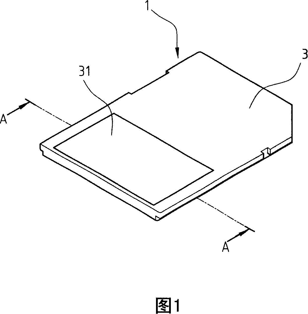
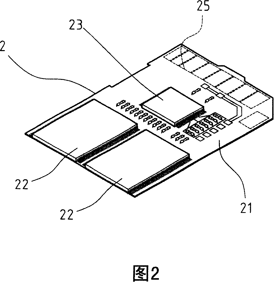
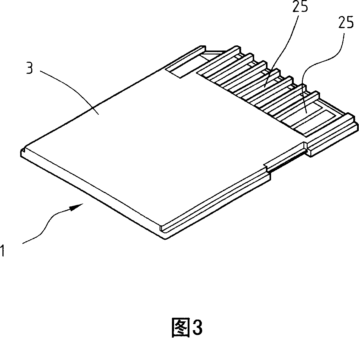
[0020] As shown in Fig. 1 and Fig. 2, they are the three-dimensional views of the structure of the memory card and the circuit board of the present invention respectively. Constituted, the first surface 21 of the circuit substrate 2 is provided with at least one memory chip 22 and a control chip 23, and the other side relative to the first surface 21 is the second surface (the bottom surface in the figure), the The second surface is provided with an electrical contact portion 25, and the inside of the circuit substrate 2 is provided with relevant circuits so that the circuits of the memory chip 22, the control chip 23 and the electrical contact portion 25 can be conducted with each other, and the electrical contact portion 25 Then, when the memory card 1 is inserted into the electronic product, it can be used as a signal transmission medium. The casing 3 is set and wrapped around the circuit board 2 to seal it inside, and the main material is ABS material (ABS, acrylintrie-but...
PUM
 Abstract
Description
Claims
Application Information