Wafer processing chamber liner and wafer processing chamber comprising same

A wafer processing and lining technology, applied in the direction of gaseous chemical plating, coating, electrical components, etc., can solve the problems of narrow protection range, inability to effectively protect and adjust the bracket, and generate thin films, so as to improve productivity and reduce downtime Cleaning time, extended protection effect

Active Publication Date: 2008-04-23
BEIJING NAURA MICROELECTRONICS EQUIP CO LTD
View PDF0 Cites 5 Cited by
  • Summary
  • Abstract
  • Description
  • Claims
  • Application Information

AI Technical Summary

Problems solved by technology

One problem with plasma etching is that when many wafers are etched in a chamber, over time a film builds up on the chamber walls
This film buildup can cause two problems: First, the film can peel off walls and infiltrate particles into the process chamber
[0006] Although the inner lining can effectively protect the inner wall of the processing chamber and the side of the wafer seat, reduce the generation of thin film accumulation, and the

Method used


Image

  • Wafer processing chamber liner and wafer processing chamber comprising same
  • Wafer processing chamber liner and wafer processing chamber comprising same
  • Wafer processing chamber liner and wafer processing chamber comprising same

Examples


Embodiment Construction

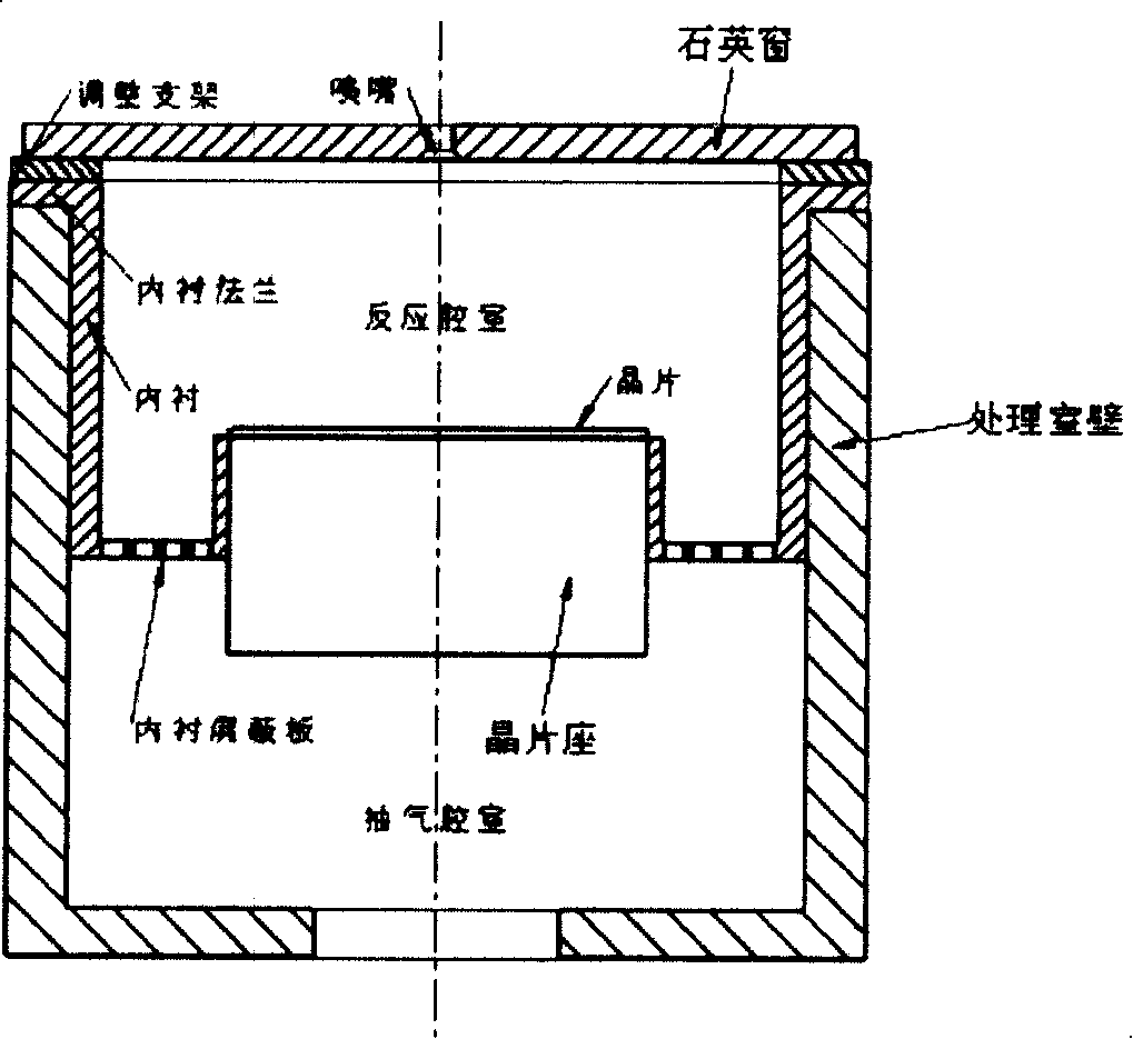
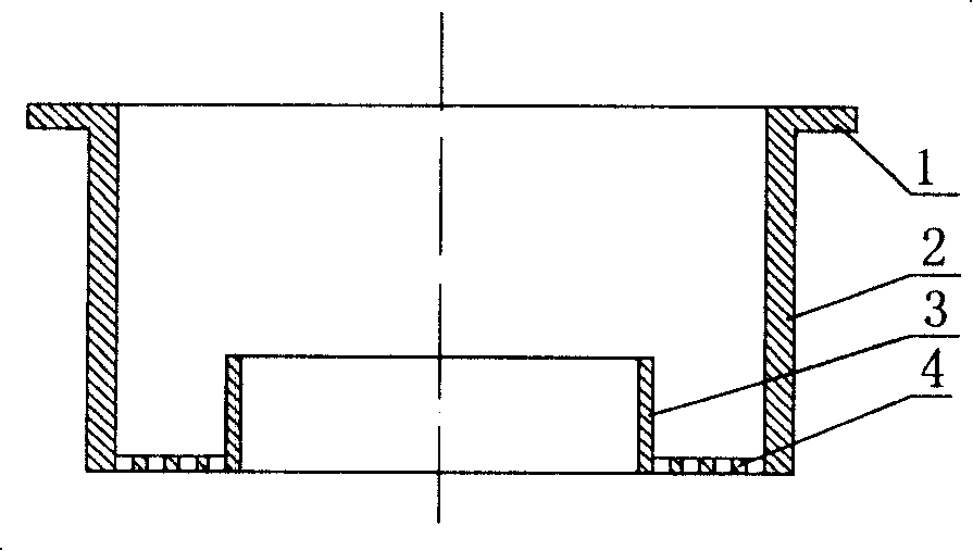
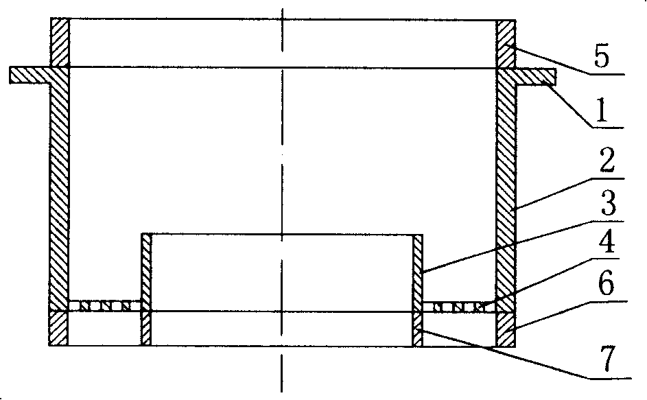
[0025] The preferred embodiment of the lining of the wafer processing chamber of the present invention is as image 3 As shown, it includes an inner wall 3 and an outer wall 2, the inner wall 3 and the outer wall 2 are connected by a shielding plate 4, the upper edge of the outer wall 2 is connected with a flange 1, and the edge of the side wall is connected with an extension part.

[0026] The extension part includes an upwardly extending part 5 of the upper edge of the outer wall 2, which is located above the upper surface of the flange 1, and is used to protect the adjustment bracket at the lower part of the quartz window. This part preferably extends upwards to the quartz window, which provides sufficient protection for the adjustment bracket.

[0027] The extended portion also includes a downwardly extending portion 6 of the lower edge of the outer sidewall 2, located below the shielding plate 4, for protecting the processing chamber wall of the pumping chamber.

[0028]...


PUM


Abstract

The internal lining comprises: inner side wall, outer side wall. The inner side wall is connected to the outer side wall through a shielding plate; the upper edge of the outer side wall is connected to a flange; the edge of side wall is connected to an extended part; said extended part comprises the part extending to upper direction of the outer side wall, the lower edge of the outer side wall, and the lower edge of the inner side wall.

Description

technical field [0001] The invention relates to a semiconductor processing equipment component, in particular to a wafer processing chamber and its lining. Background technique [0002] In semiconductor manufacturing, plasma etching of wafers is typically performed within a process chamber. One problem with plasma etching is that when many wafers are etched in a chamber, over time a film builds up on the walls of the chamber. This film buildup can cause problems in two ways: First, the film can peel off walls and infiltrate particles into the process chamber. As the device dimensions of integrated circuit devices continue to decrease, the presence of such particles during handling can increase the scrap rate of wafers. Second, the film can alter the RF ground path and thus affect the resulting wafer. [0003] In order to avoid this from happening, the chamber must be wet-cleaned periodically to wipe down the walls of the chamber to remove film buildup. However, because i...

Claims


Application Information

Patent Timeline
IPC IPC(8): H01L21/67C23F4/00
CPCH01J37/32431C23C16/44
Inventor 林盛
Owner BEIJING NAURA MICROELECTRONICS EQUIP CO LTD
Why Eureka
Try Eureka