Controlled silicon structure used for CMOS electrostatic discharge protection

An electrostatic discharge protection, silicon structure technology, applied in circuits, electrical components, electrical solid devices, etc., can solve the problems of reduced integration and large device circuit area, and achieve the effect of meeting the needs of integration.

Active Publication Date: 2008-05-07
SHANGHAI HUAHONG GRACE SEMICON MFG CORP
View PDF0 Cites 15 Cited by
  • Summary
  • Abstract
  • Description
  • Claims
  • Application Information

AI Technical Summary

Problems solved by technology

However, this design makes the circuit area of ​​the

Method used


Image

  • Controlled silicon structure used for CMOS electrostatic discharge protection
  • Controlled silicon structure used for CMOS electrostatic discharge protection
  • Controlled silicon structure used for CMOS electrostatic discharge protection

Examples


Embodiment Construction

[0016] The present invention will be described in further detail below in conjunction with the accompanying drawings.

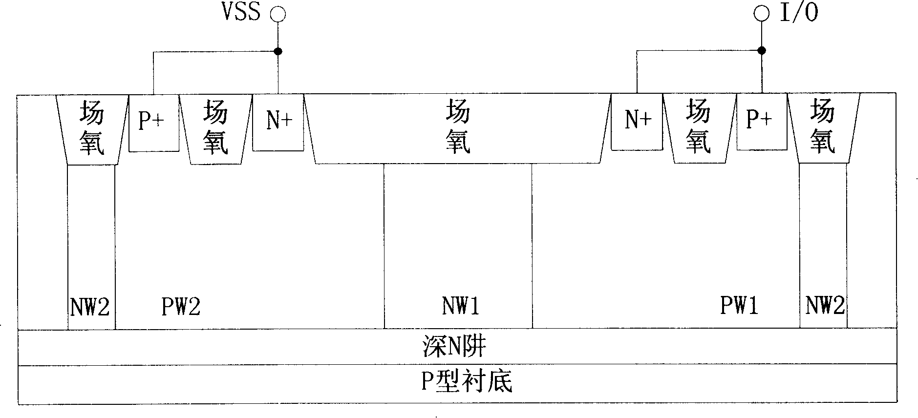
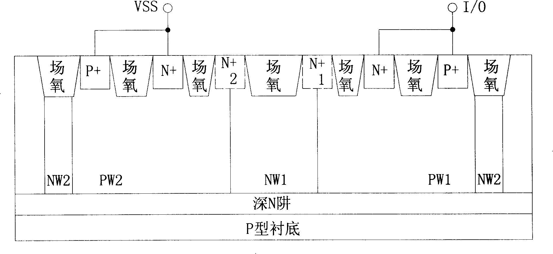
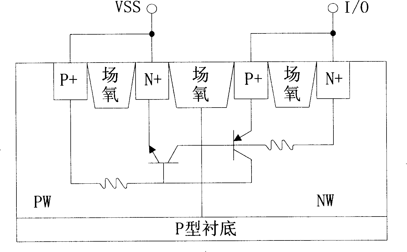
[0017] The thyristor structure used for CMOS electrostatic discharge protection in the present invention provides a novel SCR structure with bidirectional Snapback characteristics, such as figure 1 As shown, it can satisfy the requirement of CMOS electrostatic discharge protection and the requirement of integration degree at the same time. A deep N well is arranged vertically on the P-type substrate, and a second N well, a second P well, a first N well, a first P well, and a second N well are arranged in parallel on the deep N well along the lateral direction. The second P well and the first P well are respectively provided with a P+ region and an N+ region along the lateral direction, wherein the P+ region is close to the second N well, and the N+ region is close to the first N well, and each P+ region and N+ region are separated by field oxygen. In the st...


PUM


Abstract

The invention discloses a thyristor structure for CMOS static discharge protection, which is capable of both-way break-over and both-way flyback. The invention is characterized in that: a deep N well is longitudinally arranged on a P type substrate; a second N well, a second P well, a first N well, a first P well and another second N well are arranged transversely in parallel on the deep N well, and a P+ area and an N+ area are respectively transversely arranged in the second P well and the first P well in parallel; wherein, the P+ areas are close to the second N well, the N+ areas are near to the first N well, and the P+ areas and the N+ areas are divided by field oxide. The invention has the advantages of avoiding the defects in the traditional SCR structure such as single-way flyback feature, and meeting the demands for integration level.

Description

technical field [0001] The invention relates to a thyristor structure, in particular to a thyristor structure used for electrostatic discharge protection of integrated circuits. Background technique [0002] Electrostatic discharge (ESD) poses a great threat to the reliability of CMOS circuits. With the development of integrated circuits, ESD protection circuits are also continuously improved. In various ESD protection circuits, silicon controlled rectifier (SCR) has negative resistance or snapback (Snapback) characteristics and very good high current characteristics. Therefore, electrostatic protection circuits based on SCR devices are still in ultra-large-scale CMOS integrated circuits. leading position. However, the high-current characteristics of SCR devices are only good in one direction. To obtain the same protection characteristics in the other direction, only two SCR devices are connected in parallel to discharge electrostatic currents of different polarities. [...

Claims


Application Information

Patent Timeline
IPC IPC(8): H01L27/092H01L23/60
Inventor 常欣金锋
Owner SHANGHAI HUAHONG GRACE SEMICON MFG CORP
Why Eureka
Try Eureka