Flash memory device and method for controlling erased operation
A technology of flash memory and erasing voltage, applied in the field of flash memory devices
- Summary
- Abstract
- Description
- Claims
- Application Information
AI Technical Summary
Problems solved by technology
Method used
Image
Examples
Embodiment Construction
[0050] Now, various embodiments according to the present invention will be described with reference to the accompanying drawings. Since various embodiments are proposed so that those skilled in the art can understand the present invention, it can be modified in various ways and various embodiments described later do not limit the scope of the present invention.
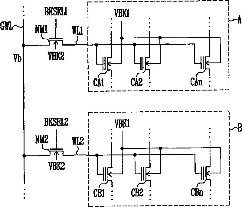
[0051] Figure 4is a block diagram of a flash memory device according to an embodiment of the present invention. The flash memory device 100 includes a memory cell array 110, an input buffer 120, a control logic circuit 130, a high voltage generator 140, an X-decoder 150, a block selection unit 160, a page buffer 170, a Y-decoder 180, and a data I / O buffer 190. The memory cell array 110 includes memory cell blocks MB1 to MBK (where K is an integer), and each memory cell block has a plurality of memory cells (not shown). The input buffer 120 receives the command signal CMD or the address signal ADD, and outputs the...
PUM
 Abstract
Description
Claims
Application Information


