Area efficient write data path circuit for SRAM yield enhancement

A circuit and write operation technology, applied in the field of memory systems, can solve the problems of SRAM memory cells unable to perform write operations, increased gate resistance of field effect transistors, and unbalanced strength.

Pending Publication Date: 2020-05-15
QUALCOMM INC
View PDF4 Cites 3 Cited by
  • Summary
  • Abstract
  • Description
  • Claims
  • Application Information

AI Technical Summary

Problems solved by technology

Additionally, smaller feature sizes may result in increased field-effect transistor (FET) performance due to short-channel effects and strength imbalance between the P-channel FET (PFET) and N-channel FET (NFET) of the SRAM memory cell. The gate resistance of
The cell write σ(sigma) of the SRAM memory cell can thus be reduced at these smaller feature sizes and result in the SRAM memory cell being unable to perform the write operation

Method used


Image

  • Area efficient write data path circuit for SRAM yield enhancement
  • Area efficient write data path circuit for SRAM yield enhancement
  • Area efficient write data path circuit for SRAM yield enhancement

Examples


Embodiment Construction

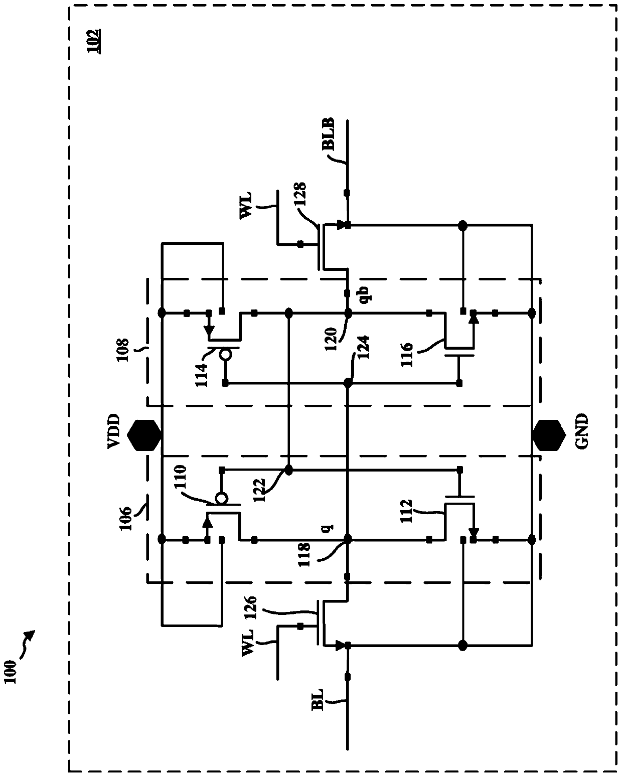
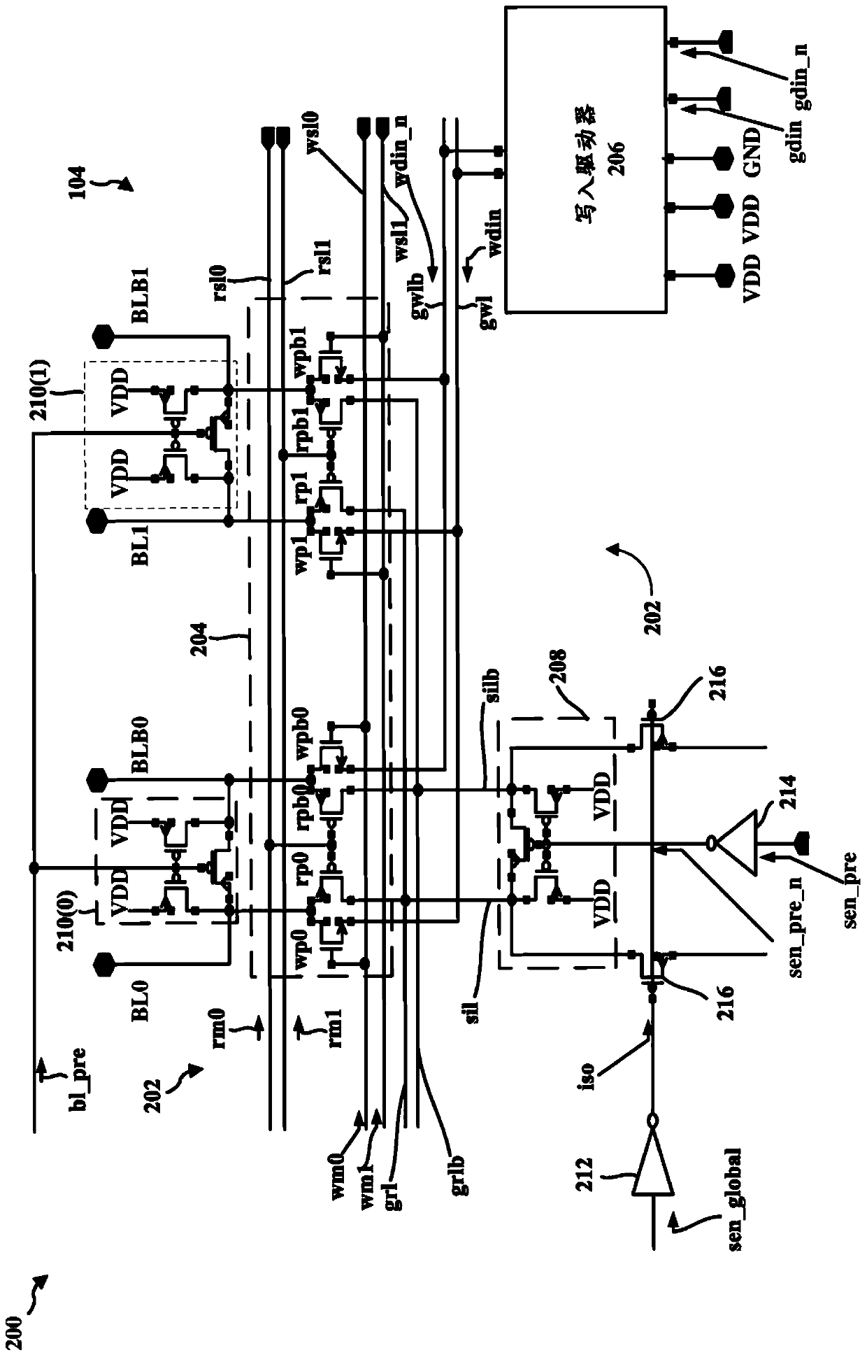
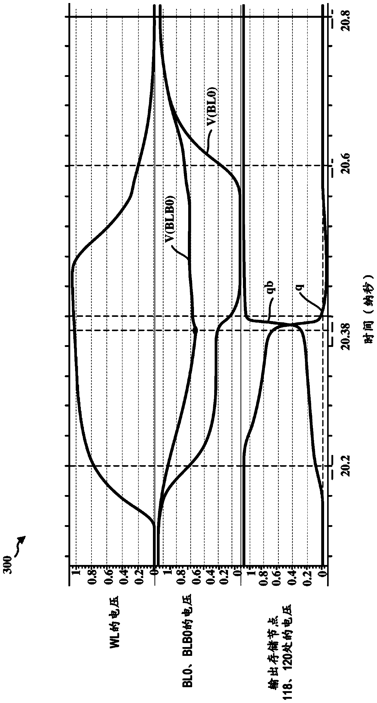
[0015] The detailed description set forth below in connection with the accompanying figures is intended as a description of various configurations and is not intended to represent the only configurations in which the concepts described herein may be practiced. The detailed description includes specific details to provide a thorough understanding of various concepts. It will be apparent, however, to one skilled in the art that these concepts may be practiced without these specific details. In some instances, well-known structures and components are shown in block diagram form in order to avoid obscuring such concepts. Acronyms and other descriptive terms may be used for convenience and clarity only and are not intended to limit any concepts disclosed herein.

[0016] The various memories presented throughout this disclosure may be implemented as stand-alone memories. Such aspects may also be included in an IC or a system / device, or a portion of an IC or a system / device (e.g.,...


PUM


Abstract

A memory and method of performing a write operation in a memory are disclosed. In one aspect of the disclosure, the memory includes a memory cell, a pair of bit lines (BL; BLB) coupled to the memory cell, a multiplexer (404), and a pull-up circuit (418) coupled to the multiplexer. The multiplexer may be configured to select the pair of bit lines coupled to the memory cell during the write operation. To increase the write performance of the memory cell, the pull-up circuit is configured to select which of the pair of bit lines is a non zero bit line during the write operation and to clamp thenon-zero bit line through read pass transistors (rpO, rpbO) of the multiplexer to approximately a power rail voltage (VDD). Thus, the pull-up circuit (418) may increase the voltage difference betweenthe non-zero bit line and the zero bit line during the write operation and thus decrease the area and power consumed by a boost capacitance of a conventional write driver.

Description

[0001] Cross References to Related Applications [0002] This patent application claims priority to U.S. Nonprovisional Application No. 15 / 727,448, filed October 6, 2017, entitled "AREA EFFICIENT WRITE DATAPATH CIRCUIT FOR SRAM YIELD ENHANCEMENT," which is assigned to this application assignee and is hereby expressly incorporated by reference. technical field [0003] The present disclosure relates generally to memory systems, and more particularly to apparatuses including memory systems for performing write operations. Background technique [0004] As integrated circuit (IC) technology advances, semiconductor fabrication processes continue to shrink feature sizes and provide denser ICs. This trend continues to prevail in memories used to store data in digital processing systems. In general, memory can store more and more data in a given area of ​​an IC as feature sizes decrease. However, smaller feature sizes can also lead to increased variation in resistive characteris...

Claims


Application Information

Patent Timeline
Patent Type & Authority Applications(China)
IPC IPC(8): G11C7/12G11C11/419
CPCG11C7/12G11C11/419
Inventor S·K·古普塔P·拉杰R·萨胡M·纳拉西姆汉
Owner QUALCOMM INC
Why Eureka
Try Eureka