Display substrate and display device

A display substrate and substrate technology, applied in optics, instruments, character and pattern recognition, etc., can solve problems such as weak charge signal and affecting fingerprint recognition effect

Pending Publication Date: 2021-02-19
BOE TECH GRP CO LTD +1
View PDF6 Cites 3 Cited by
  • Summary
  • Abstract
  • Description
  • Claims
  • Application Information

AI Technical Summary

Problems solved by technology

However, due to the small amount of charge in the capacitor in the capacitive fingerprint recognition unit, the charge signal formed by the capacitor is weak, which affects the fingerprint recognition effect.

Method used


Image

  • Display substrate and display device
  • Display substrate and display device
  • Display substrate and display device

Examples


Embodiment Construction

[0031] The specific implementation manners of the present invention will be further described in detail below in conjunction with the accompanying drawings and examples. The following examples are used to illustrate the present invention, but are not intended to limit the scope of the present invention. It should be noted that, in the case of no conflict, the embodiments in the present application and the features in the embodiments can be combined arbitrarily with each other.

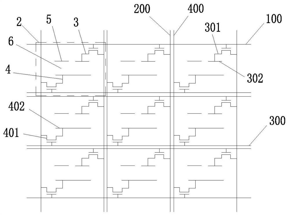
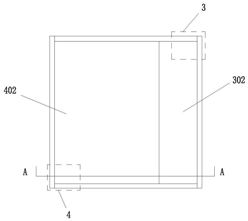
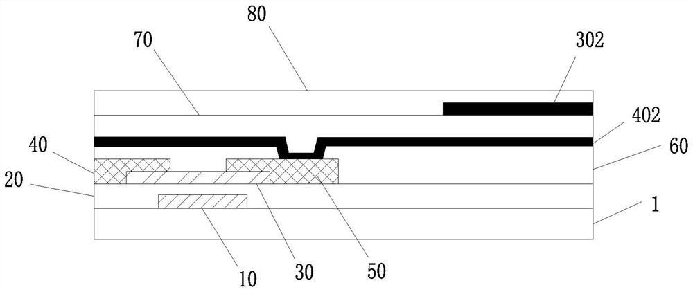
[0032] An embodiment of the present invention provides a display substrate, including a substrate and a fingerprint recognition unit disposed on the substrate, the fingerprint recognition unit includes an excitation circuit and a reading circuit, and the reading circuit is configured to communicate with the fingerprint to be recognized forming a first capacitor and reading a charge signal of the first capacitor, the excitation circuit includes a first thin film transistor and a first electrode plate co...


PUM


Abstract

The embodiment of the invention provides a display substrate and a display device, the display substrate comprises a substrate and a fingerprint identification unit arranged on the substrate, and thefingerprint identification unit comprises an excitation circuit and a reading circuit. The reading circuit is configured to form a first capacitor with a fingerprint to be identified and read a chargequantity signal of the first capacitor, and the excitation circuit comprises a first thin film transistor and a first electrode plate connected with the first thin film transistor. the first thin film transistor is configured to apply a driving voltage to the first electrode plate, and the first electrode plate is configured to boost the voltage of the fingerprint to be identified through the driving voltage; and the fingerprint identification effect is improved.

Description

technical field [0001] The present invention relates to the field of display technology, in particular to a display substrate and a display device. Background technique [0002] The liquid crystal display device is a display device used on a large scale at present. It has the advantages of high color gamut, lightness and thinness, and fast response time. It has mature technologies in theoretical research and practical technology. [0003] Fingerprint identification technology is to match a person with his fingerprint, and verify his real identity by comparing his fingerprint with the pre-saved fingerprint. Each person's (including fingerprints) skin texture is unique in patterns, breakpoints and intersections. Relying on this uniqueness and stability, fingerprint recognition technology is realized. Fingerprint recognition technology is mainly used in consumer electronics such as mobile phones and personal computers, smart door locks in smart homes, and fingerprint cards in ...

Claims


Application Information

Patent Timeline
Patent Type & Authority Applications(China)
IPC IPC(8): G02F1/1333G02F1/1343G02F1/1362G06K9/00
CPCG02F1/13338G02F1/136286G02F1/134309G06V40/1318
Inventor 庞凤春李月曹雪肖月磊吴艺凡常文博
Owner BOE TECH GRP CO LTD
Why Eureka
Try Eureka