In-tray inspection apparatus and method of semiconductor package

An inspection method and inspection equipment technology, applied in the direction of single semiconductor device testing, measuring devices, instruments, etc., can solve problems such as increased operating costs and difficulties, and achieve the effects of improving efficiency and reducing the time required for inspection

Active Publication Date: 2008-05-28
INTEKPLUS
View PDF0 Cites 2 Cited by
  • Summary
  • Abstract
  • Description
  • Claims
  • Application Information

AI Technical Summary

Problems solved by technology

[0011] However, as described above, when the visual probe is fixed in a predetermined direction to perform visual inspection of the semiconductor package, since the arrangement direction of the pins of the semiconductor package varies according to the type of the semiconductor package to be inspected, for example, The pins are arranged in the lateral direction of the semiconductor package in the thin small outline package 1 (TSOP1), and the leads are arranged in the longitudinal direction of the semiconductor package in the thin small outline package 2 (TSOP2) different from the TSOP1 type, and The pins at the periphery of the semiconductor package are arranged in a QFP type, so it is practically impossible to perform visual inspection of various types of semiconductor packages using a single inspection device
[0012] Therefore, it is difficult to use specific inspection equipment so that its visible probes are mounted in the directions required for various types of semiconductor packages.
In addition, since additional inspection equipment with the same inspection function must be purchased, operating costs are increased

Method used


Image

  • In-tray inspection apparatus and method of semiconductor package
  • In-tray inspection apparatus and method of semiconductor package
  • In-tray inspection apparatus and method of semiconductor package

Examples


Embodiment Construction

[0022] Hereinafter, preferred embodiments of the present invention will be described in detail with reference to the accompanying drawings so that those skilled in the art can easily understand and implement the present invention.

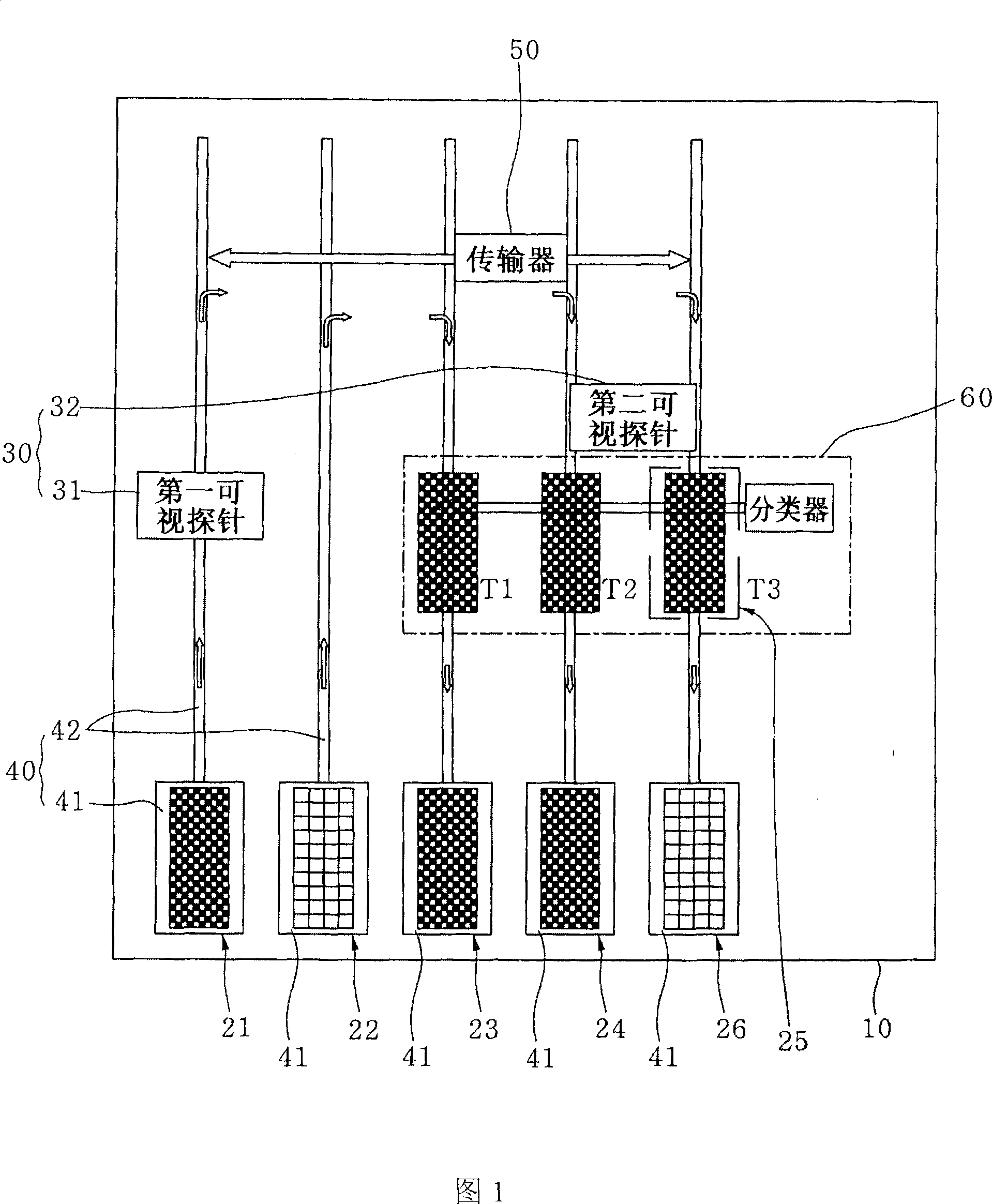
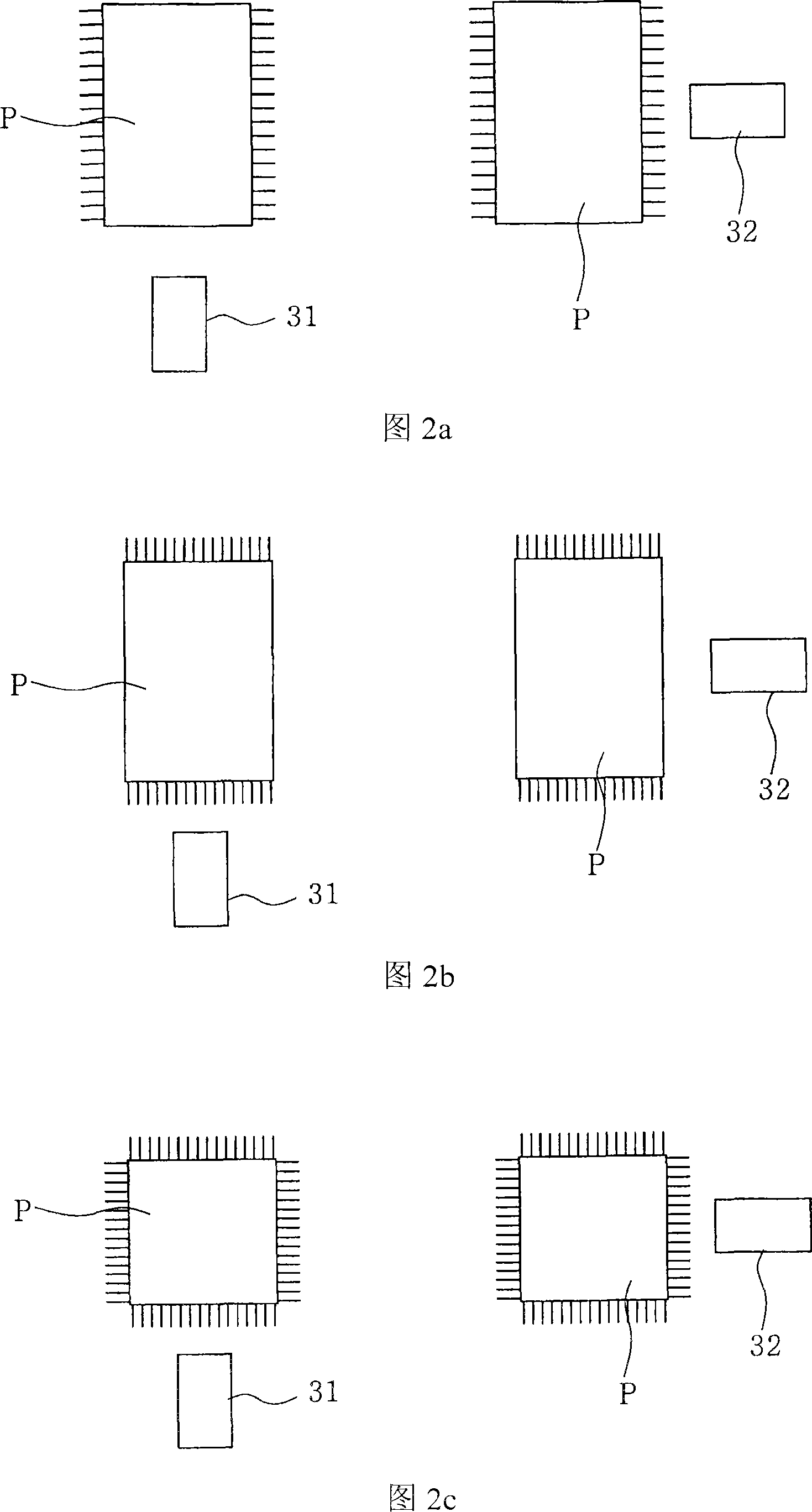
[0023] FIG. 1 is a schematic diagram showing an inspection device according to a preferred embodiment of the present invention, and FIG. 2 is a diagram showing an arrangement of visual probes of the inspection device according to a preferred embodiment of the present invention.

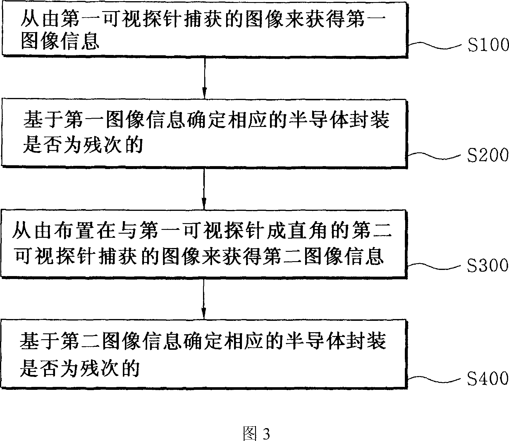
[0024] As shown in FIG. 1 , an in-disk inspection apparatus according to a preferred embodiment of the present invention includes an inspector 30 disposed on a transfer path of a reel (hereinafter referred to as "inspected object") for accommodating semiconductor packages. to photograph the appearance of the object, and the central controller (not shown) is used to compare the image information of the object obtained by the inspector 30 with reference image information of a...


PUM


Abstract

The present invention relates to an apparatus and method for inspecting the appearance of a semiconductor package, and more particularly to an in-panel apparatus for inspecting a semiconductor package to shorten a tray according to the semiconductor package during the in-panel inspection. Improve efficiency and reliability by reducing inspection time of internal semiconductor packages and minimizing disturbances caused by shadows created by projected beams. The apparatus includes first and second visual probes positioned on a transport path of semiconductor packages housed in a tray, and a central controller that correlates image information obtained by the visual probes with information about corresponding The reference image information of different types of semiconductor packages is compared to analyze and determine whether the semiconductor package is defective. The first visible probe is parallel to a track direction in which the disk is transported, and the second visible probe is arranged at a predetermined angle to the first visible probe.

Description

technical field [0001] The present invention relates to an apparatus and method for inspecting the appearance of a semiconductor package, and more particularly, to an apparatus for inspecting an in-panel semiconductor package in which the semiconductor package contained in the The time required for inspection of semiconductor packages in the tray is shortened, and disturbance due to shadows created by projected beams is minimized to improve efficiency and reliability. Background technique [0002] A semiconductor device must be accurately inspected after it is manufactured by a manufacturing process and is about to be shipped. If the inside of the packaged semiconductor device is defective or the exterior of the package is slightly defective, the defective portion has a serious influence on the semiconductor device. [0003] Inspection of leads of semiconductors such as quad flat packages (QFPs) is a very important process since external defects such as defects of semicondu...

Claims


Application Information

Patent Timeline
Patent Type & Authority Applications(China)
IPC IPC(8): G01R31/26
CPCG01R31/2896
Inventor 李相允崔二培姜珉求林双根
Owner INTEKPLUS
Why Eureka
Try Eureka