Light emitting diode package, and light source unit and backlight unit including the same

A technology of light-emitting diodes and light source units, which is applied to optical elements, light sources, electric light sources, etc., which are used to change the spectral characteristics of emitted light, and can solve the problems of weakened light brightness and enlarged external dimensions

Inactive Publication Date: 2008-06-11
SAMSUNG ELECTRONICS CO LTD
View PDF0 Cites 13 Cited by
  • Summary
  • Abstract
  • Description
  • Claims
  • Application Information

AI Technical Summary

Problems solved by technology

Therefore, the external size of the display device becom

Method used


Image

  • Light emitting diode package, and light source unit and backlight unit including the same
  • Light emitting diode package, and light source unit and backlight unit including the same
  • Light emitting diode package, and light source unit and backlight unit including the same

Examples


Embodiment Construction

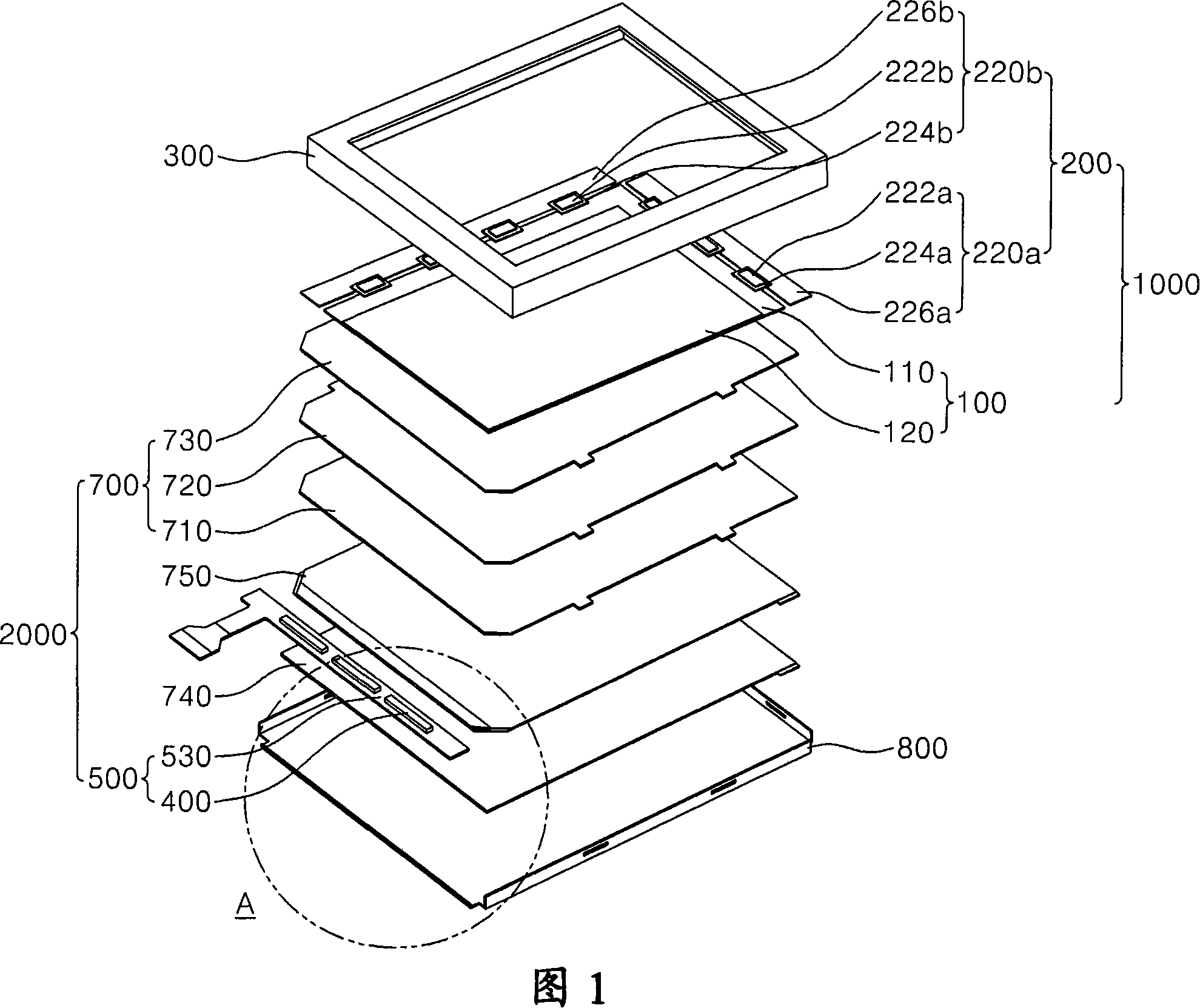
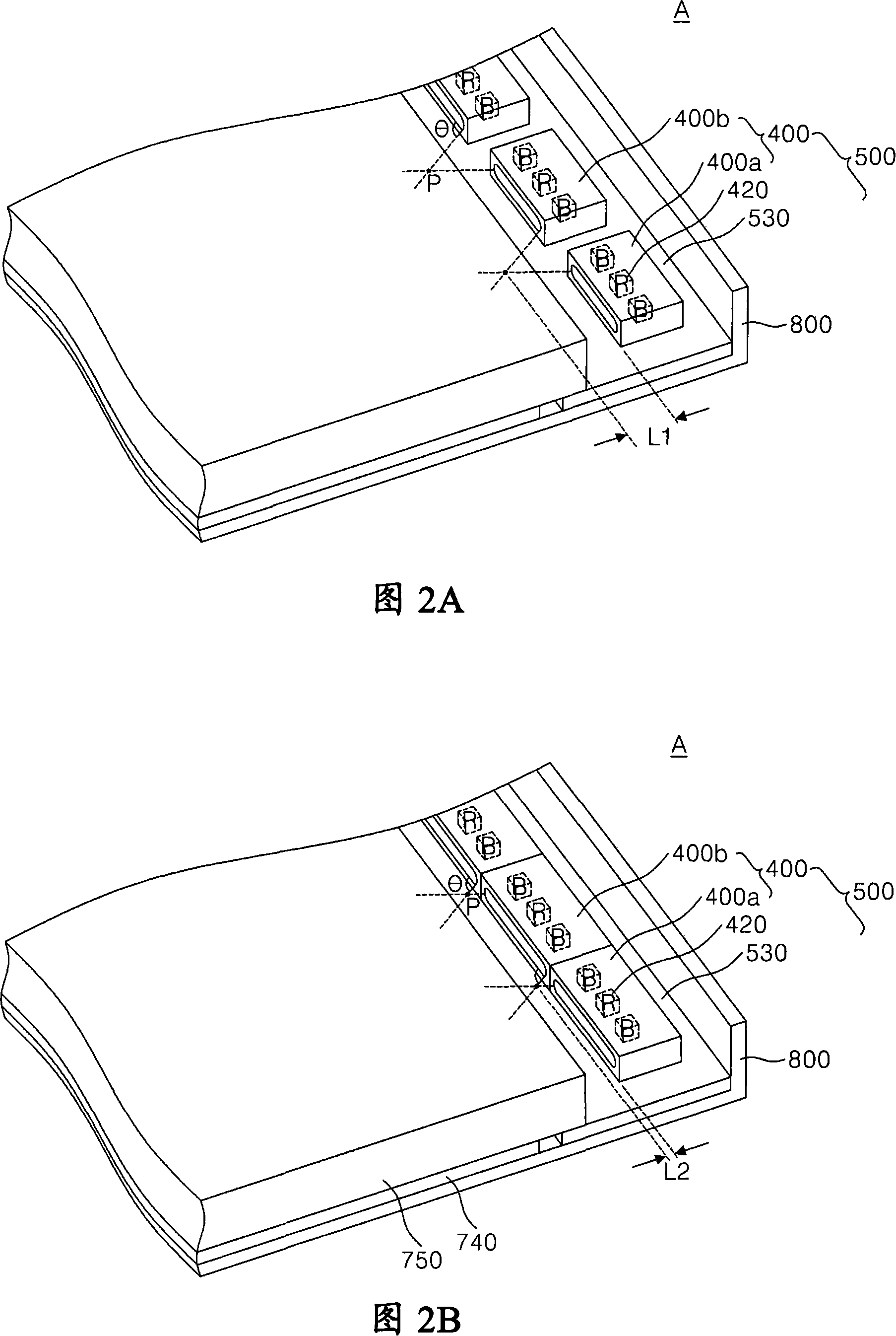
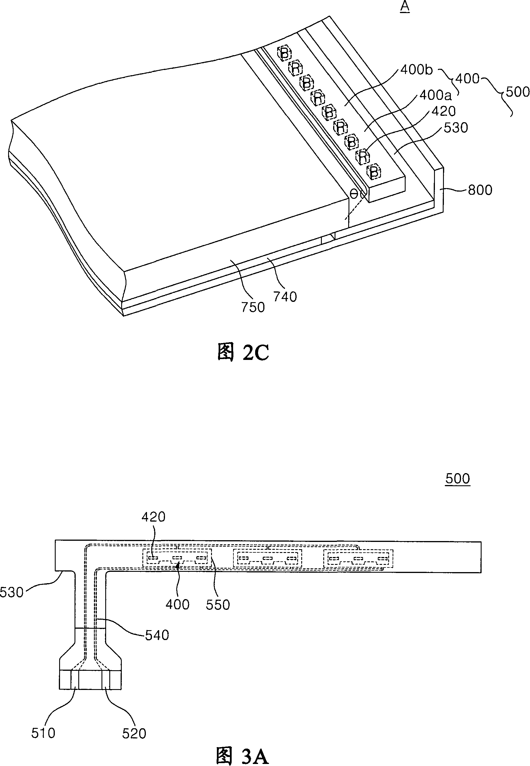
[0033] The present invention will now be described more fully with reference to the accompanying drawings that illustrate embodiments of the invention. However, this invention may be embodied in different forms and should not be construed as limited to only the embodiments set forth herein. Of course, these embodiments are provided so that this disclosure will be thorough and complete, and will fully convey the scope of the invention to those skilled in the art. Throughout the specification, the same reference numerals denote the same elements.

[0034] It will be understood that when an element is referred to as being "on" another element, it can be directly on the other element or intervening elements may be present therebetween. In contrast, when an element is referred to as being "directly on" another element, there are no intervening elements present. As used herein, the term "and / or" includes any and all combinations of one or more of the associated listed items.

[0...


PUM


Abstract

The light emitting diode ("LED") package includes at least one LED chip which emits light, a housing defining a space for receiving the at least one LED chip, and the housing including a light emitting surface which collects the light emitted from the at least one LED chip and emits the same to an external environment and a lead portion, penetrating a lower surface of the housing, one end of the lead portion is electrically connected to the at least one LED chip in the housing and another end of the lead portion is exposed to the external environment.

Description

[0001] This application claims priority and all benefits under 35 U.S.C § 119 of Korean Patent Application No. 2006-0121956 filed on December 5, 2006, the disclosure of which is hereby incorporated by reference in its entirety. technical field [0002] The present invention relates to a liquid crystal display (LCD) device, and more particularly, to a light emitting diode (LED) package capable of reducing the outer size of an LCD panel by minimizing the generation of hot spots and the distance of dead zones and including the A light source unit and a backlight unit of an LED package. Background technique [0003] In general, LCD devices display images using electrical and optical properties of liquid crystals. LCD devices are used in various applications such as portable computers, communication equipment, liquid crystal televisions, etc. due to their advantages such as compactness and light weight compared to cathode ray tubes (CRTs). [0004] The LCD device includes a liqu...

Claims


Application Information

Patent Timeline
IPC IPC(8): H01L25/00H01L25/075H01L33/00H01L23/04H01L23/48F21K7/00F21S8/00F21V3/02G02F1/13357F21Y101/02F21S2/00F21V8/00F21V9/16G02F1/1335H01L33/48H01L33/50H01L33/62
CPCH01L25/0753G02B6/0068H01L2224/48237H01L33/62H01L33/50G02B6/0073H01L2224/48091H01L2224/73265H01L2224/48227H01L2224/32225H01L24/73H01L2924/00014H01L2924/00H01L2924/00012
Inventor 申东烈全孝锡崔在镇郭容硕金大燮
Owner SAMSUNG ELECTRONICS CO LTD
Why Eureka
Try Eureka