Light emitting element, light emitting device and electronic apparatus

A technology for light-emitting devices and light-emitting layers, applied in electrical components, electric solid-state devices, semiconductor devices, etc., can solve problems such as operating failures of light-emitting components, and achieve the effect of reducing unevenness and excellent color.

Active Publication Date: 2008-06-18
SEMICON ENERGY LAB CO LTD
View PDF2 Cites 17 Cited by
  • Summary
  • Abstract
  • Description
  • Claims
  • Application Information

AI Technical Summary

Problems solved by technology

[0005] It is conceivable that the technology mentioned in Patent Document 1 is also effective; however, molybdenum oxide is easily crystallized, and therefore in the technology mentioned in Patent Document 1, there is a tendency for the problem of operational failure of the light-emitting element due to crystallization

Method used


Image

  • Light emitting element, light emitting device and electronic apparatus
  • Light emitting element, light emitting device and electronic apparatus
  • Light emitting element, light emitting device and electronic apparatus

Examples


Embodiment approach 1

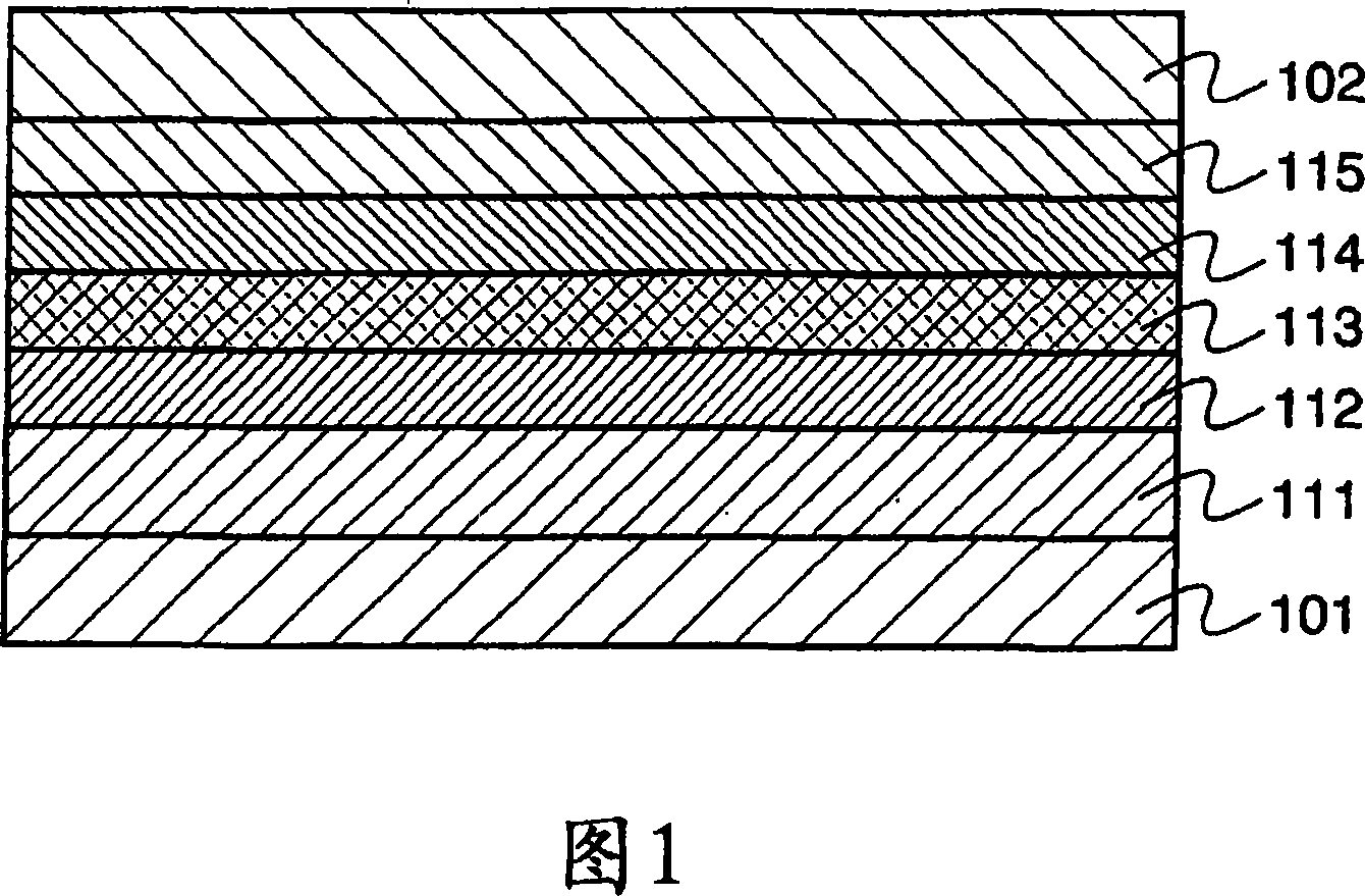
[0041] One mode of the light-emitting element of the present invention will be described with reference to FIG. 1 .

[0042] FIG. 1 shows a light emitting element having a light emitting layer 113 between a first electrode 101 and a second electrode 102 . In the light emitting element shown in FIG. 1 , the mixed layer 111 is provided between the light emitting layer 113 and the first electrode 101 . The hole transport layer 112 is disposed between the light emitting layer 113 and the mixing layer 111 , and the electron transport layer 114 and the electron injection layer 115 are disposed between the light emitting layer 113 and the second electrode 102 . In such a light-emitting element, when a voltage is applied to the first electrode 101 and the second electrode 102 so that the potential of the first electrode 101 is higher than the potential of the second electrode 102, holes are injected from the side of the first electrode 101 to emit light. In the layer 113, electrons a...

Embodiment approach 2

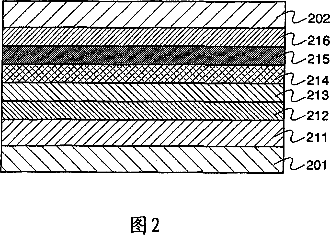
[0061] One mode of the light emitting element of the present invention is described with reference to FIG. 2 .

[0062] 2 shows a light emitting element with a light emitting layer 213, a first mixed layer 215 and a second mixed layer 216 between the first electrode 201 and the second electrode 202, wherein the light emitting layer 213 is closer to the first mixed layer than the first mixed layer 215. For the electrode 201 , the second mixed layer 216 is closer to the second electrode 202 than the first mixed layer 215 . In this light emitting element, the hole injection layer 211 and the hole transport layer 212 are provided between the light emitting layer and the first electrode 201 , and the electron transport layer 214 is provided between the light emitting layer 213 and the first mixed layer 215 . The first mixed layer 215 is a layer including an electron transport substance and one substance selected from alkaline metals, alkaline earth metals, alkaline metal oxides, al...

Embodiment approach 3

[0079]Next, one mode of the light-emitting element of the present invention will be described with reference to FIG. 20 . FIG. 20 shows a light emitting element having a plurality of light emitting layers, specifically a first light emitting layer 413a, a second light emitting layer 413b, and a third light emitting layer 413c between the first electrode 401 and the second electrode 402. This light-emitting element has a first mixed layer 421a and a second mixed layer 422a between the first light-emitting layer 413a and the second light-emitting layer 413b, and has a first mixed layer 421b between the second light-emitting layer 413b and the third light-emitting layer 413c. and the second mixed layer 422b. The first mixed layer 421a, 421b is a layer including an electron transport substance and a substance selected from alkaline metals, alkaline earth metals, alkaline metal oxides, alkaline earth metal oxides, alkaline metal fluorides, and alkaline earth metal fluorides. . Th...


PUM


Abstract

One aspect of the present invention is a light-emitting element having a layer containing an aromatic hydrocarbon and a metal oxide between a pair of electrodes. There is no particular limitation on the kind of aromatic hydrocarbon; however, an aromatic hydrocarbon having a hole mobility of 1 x 10⁻⁶ cm2 / Vs or more is preferable. Examples of such aromatic hydrocarbons include 2-tert-butyl-9,10-bis(2-naphthyl)anthracene, anthracene, 9,10-diphenylanthracene, tetracene, rubrene, perylene, 2,5,8,11-tetra(tert-butyl)perylene and so on. As the metal oxide, a metal oxide exhibiting electron-accepting properties for aromatic hydrocarbons is preferable. As such metal oxides, for example, molybdenum oxide, vanadium oxide, ruthenium oxide, rhenium oxide and the like are given.

Description

technical field [0001] The present invention relates to a light-emitting element having a layer containing a light-emitting substance between electrodes, and to a light-emitting device and electronic equipment having the light-emitting element. Background technique [0002] A light-emitting element that has attracted attention as a pixel of a display device or a light source of a lighting device in recent years has a light-emitting layer between electrodes, and a light-emitting substance contained in the light-emitting layer emits light when a current flows between the electrodes. [0003] In the field of research and development of such light-emitting elements, one of the important purposes is to prolong the service life of the light-emitting elements. This is because a light emitting element provided for a light emitting device needs to operate satisfactorily for a long time in order to use a light emitting device such as a lighting device or a display device under satisfa...

Claims


Application Information

Patent Timeline
Patent Type & Authority Applications(China)
IPC IPC(8): H01L51/50
CPCH01L51/5048H10K50/14H10K85/615
Inventor 岩城裕司濑尾哲史川上贵洋池田寿雄坂田淳一郎
Owner SEMICON ENERGY LAB CO LTD
Why Eureka
Try Eureka