Motherboard of display panel and production method thereof

A technology for display panels and manufacturing methods, which is applied in semiconductor/solid-state device manufacturing, optics, instruments, etc., can solve problems such as the limitation of motherboard utilization, and achieve the effect of improving motherboard utilization and increasing production capacity

Active Publication Date: 2008-07-16
AU OPTRONICS CORP
View PDF0 Cites 9 Cited by
  • Summary
  • Abstract
  • Description
  • Claims
  • Application Information

AI Technical Summary

Problems solved by technology

[0007] The technical problem to be solved by the present invention is to provide a motherboard of a display panel, which can effectively utilize the available space on the motherboard and solve the problem that the utilization rate of the motherboard is limited

Method used


Image

  • Motherboard of display panel and production method thereof
  • Motherboard of display panel and production method thereof
  • Motherboard of display panel and production method thereof

Examples


Embodiment Construction

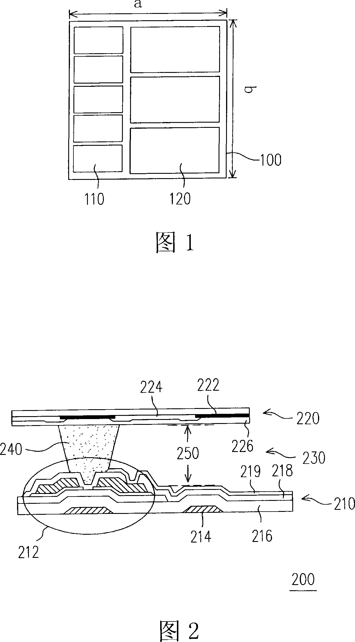
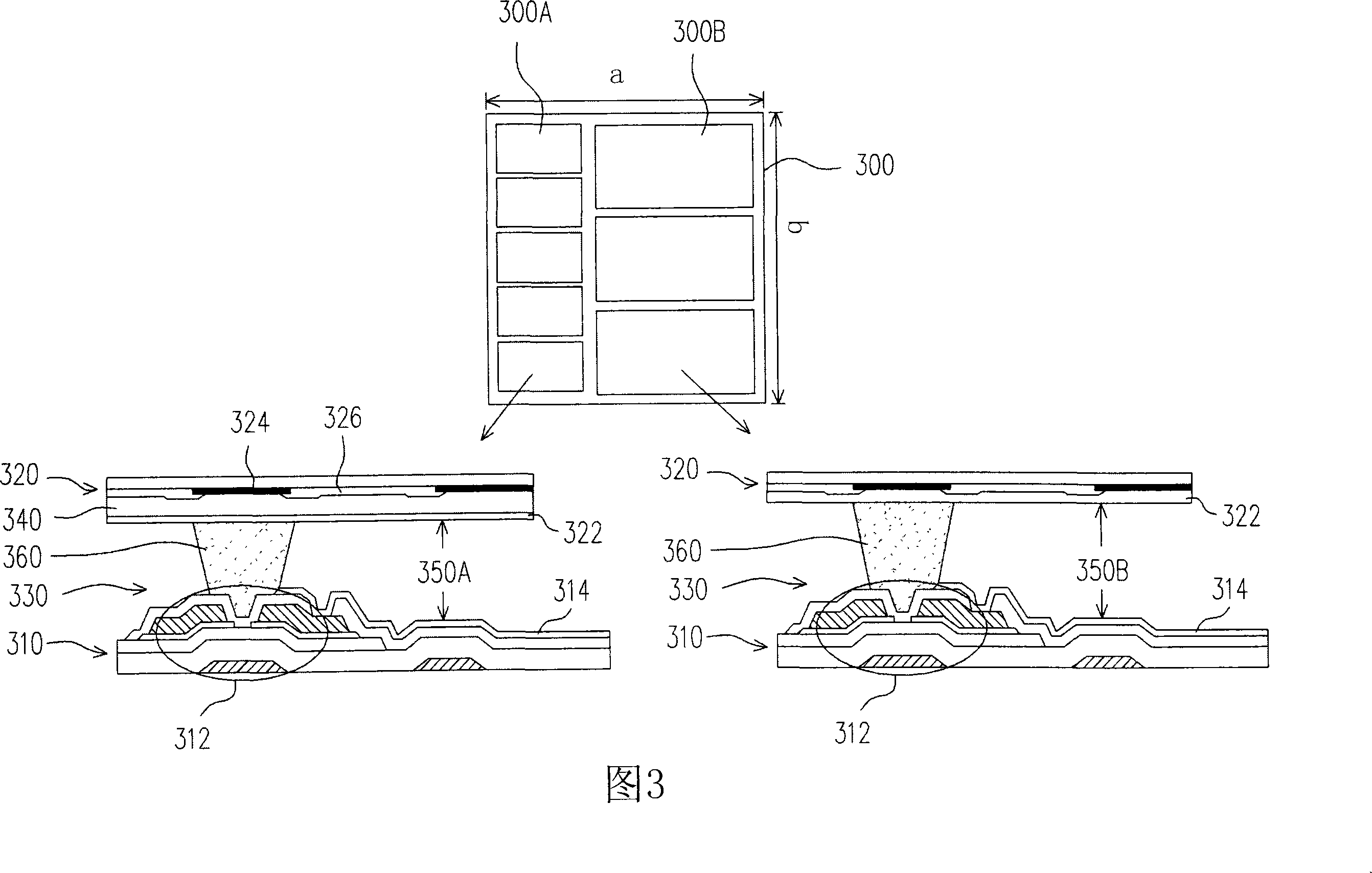
[0036] The motherboard mentioned in the following embodiments refers to the assembly of a whole piece of switching element array substrate and a whole piece of counter substrate, and sealing the display medium layer between them, forming a plurality of panels Finished unit. Cutting the motherboard can form multiple independent display panels.

[0037] These embodiments do not limit the type of the display panel, and the display panel has different action mechanisms with different display medium layers. For example, the display medium layer can be a liquid crystal material, and the display panel is called a liquid crystal display panel, such as: a transmissive display panel, a semi-transmissive display panel, a reflective display panel, a COA display panel, an AOC display panel, a vertical Alignment (VA) Display Panel, Horizontal Switching (IPS) Display Panel, Multi-Domain Vertical Alignment (MVA) Display Panel, Twisted Nematic (TN) Display Panel, Super Twisted Nematic (STN) D...


PUM


Abstract

The invention discloses a mother board of a display panel and a method for making the same, wherein the mother board has first panel cells and second panel cells which are different in size and are provided with different cell gaps. The mother board is mainly composed of a switchover element array substrate, a counter substrate, a display medium layer and an underlayer. The switchover element array substrate is provided with a plurality of switchover elements which are arranged in an array and a plurality of pixel electrodes correspondingly connected with the switchover elements. The counter substrate is actually parallel to the switchover elements. The display medium layer is arranged between the switchover element array substrate and the counter substrate. The underlayer is arranged between the switchover element array substrate and the counter substrate and is corresponding to the first panel cells for compensating for the cell gaps between the first panel cells and the second panel cells.

Description

technical field [0001] The invention relates to a motherboard of a display panel and a manufacturing method thereof, in particular to a motherboard with display panel units of different sizes and a manufacturing method thereof. Background technique [0002] The liquid crystal display is mainly composed of a liquid crystal display panel (LCD panel) and a backlight module (backlight module), wherein the liquid crystal display panel includes a color filter substrate, an active device array substrate (active device array substrate) and a liquid crystal layer located between the two substrates. [0003] The production of the current liquid crystal display panel is to first assemble a whole piece of active element array substrate and a whole piece of color filter substrate, and seal the liquid crystal layer between them, and then form a liquid crystal display panel with a plurality of panel units motherboard. Afterwards, the motherboard of the liquid crystal display panel is cut...

Claims


Application Information

Patent Timeline
Patent Type & Authority Applications(China)
IPC IPC(8): G02F1/136G02F1/1335G02F1/1333H01L27/12H01L21/84
Inventor 黄彦衡陈宗凯李淑琴
Owner AU OPTRONICS CORP
Why Eureka
Try Eureka