Pixel structure

A pixel structure and pixel electrode technology, which is applied to the field of pixel structures with multi-channel regions, can solve the problems such as the limitation of the display aperture ratio of the pixel structure, and achieve the effects of avoiding the influence of the display aperture ratio and reducing the leakage current.

Active Publication Date: 2010-12-08
AU OPTRONICS CORP
View PDF3 Cites 1 Cited by
  • Summary
  • Abstract
  • Description
  • Claims
  • Application Information

AI Technical Summary

Problems solved by technology

[0005] The technical problem to be solved by the present invention is to provide a pixel structure to solve the problem that the display aperture ratio of the pixel structure is limited by the multi-channel design of polysilicon thin film transistors

Method used


Image

  • Pixel structure
  • Pixel structure
  • Pixel structure

Examples


Embodiment Construction

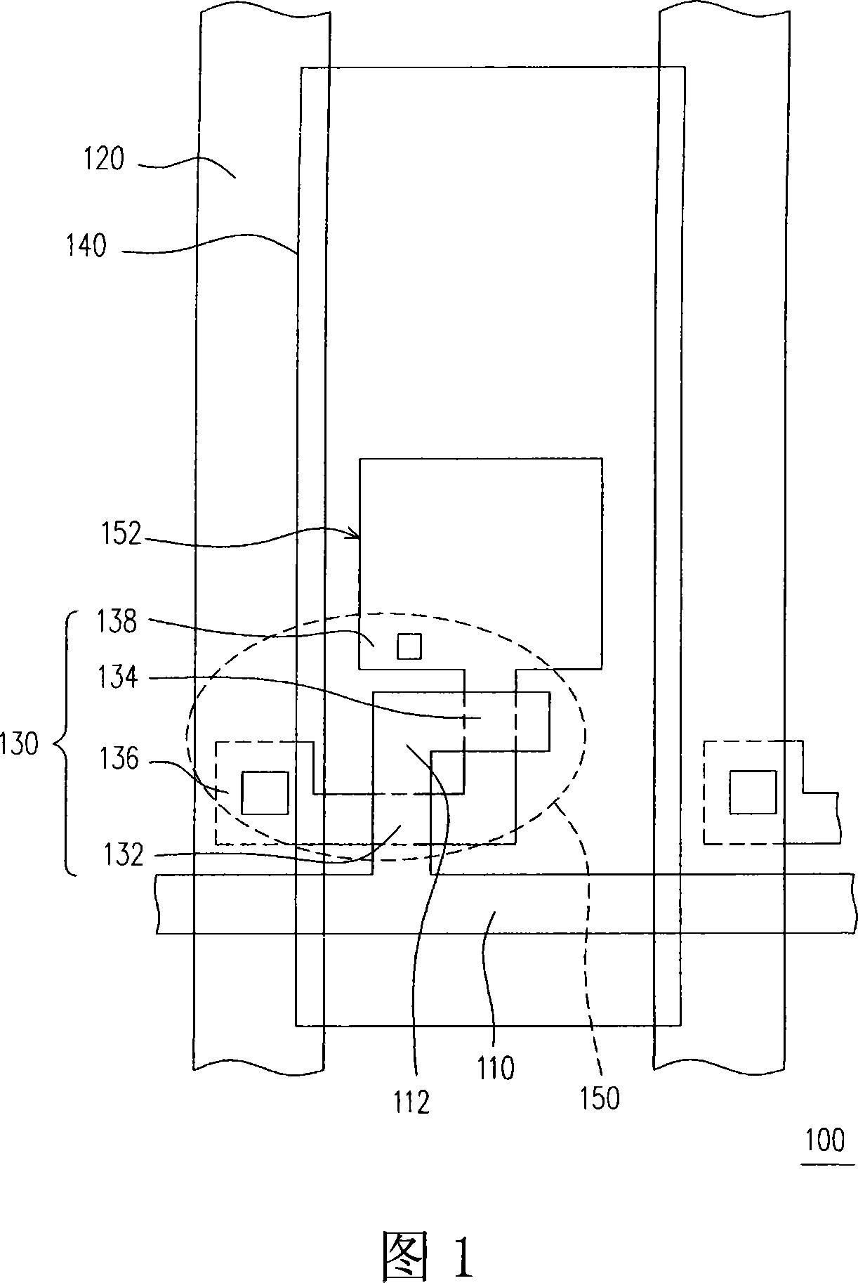
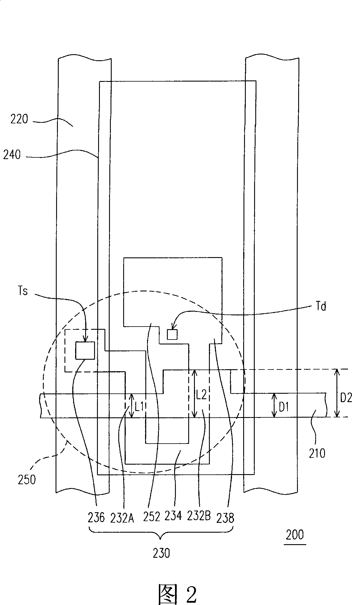
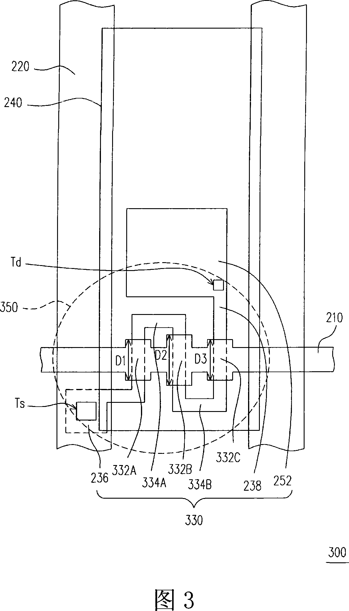
[0048] figure 2 It is a pixel structure of an embodiment of the present invention. Please refer to figure 2 , the pixel structure 200 is electrically connected to a scan line 210 and a data line 220, wherein the scan line 210 and the data line 220 are arranged alternately. The pixel structure 200, the scan lines 210 and the data lines 220 are, for example, disposed on a substrate (not shown). The pixel structure 200 includes a semiconductor pattern 230 and a pixel electrode 240 . The semiconductor pattern 230 includes at least two channel regions 232A, 232B, at least one doped region 234 , and a source region 236 and a drain region 238 . The channel regions 232A and 232B are located under the scan line 210 , wherein the channel region 232A and the channel region 232B have different width-to-length ratios. The doped region 234 is connected between the channel region 232A and the channel region 232B. The pixel electrode 240 is electrically connected to the drain region 23...


PUM


Abstract

The invention discloses a pixel structure which is arranged on a substrate and electrically connected with a scanning wire and a data line, wherein, the pixel comprises a semi-conductor pattern and a pixel electrode. The semi-conductor pattern comprises at least two channel regions, at least one doped region and a source electrode region as well as a drain electrode region. The channel regions are positioned below the scanning wire, wherein, the channel regions have different width / length ratios. The doped region is connected between the channel regions. The pixel electrode is electrically connected with the drain electrode region, wherein, the source electrode region is connected between one of the channel regions and the data line, and the drain electrode region is connected between theother channel region and the pixel electrode. The scanning wires above different channel regions have different widths, and the length of each channel region is equal to the width of the scanning wire.

Description

technical field [0001] The present invention relates to a pixel structure, and in particular to a pixel structure with a multi-channel area. Background technique [0002] Thin Film Transistor Liquid Crystal Display (TFT-LCD) has become the mainstream of many flat panel displays at present. According to the selection of the material of the channel layer, TFT-LCDs can be divided into two types: amorphous silicon TFT-LCDs and low-temperature polysilicon thin-film transistors (Low-Temperature PolySilicon Thin FilmTransistor, LTPS-TFT) LCDs. [0003] Since the electron mobility of low-temperature polysilicon thin film transistors can reach 200cm 2 / V-sec or more, so the area occupied by the TFT element can be made smaller to meet the requirement of high aperture ratio (aperture), thereby improving the display brightness of the display and reducing the overall power consumption problem. But relatively speaking, low-temperature polysilicon thin film transistors also have a relati...

Claims


Application Information

Patent Timeline
Patent Type & Authority Patents(China)
IPC IPC(8): H01L27/12H01L23/522G02F1/136G02F1/1362
Inventor 萧嘉强罗诚胡至仁
Owner AU OPTRONICS CORP
Why Eureka
Try Eureka