Power semiconductor device

A technology of power semiconductors and semiconductors, which is applied in the direction of semiconductor devices, circuits, electrical components, etc., can solve the problems of large amount of metal film etching, low etching precision, and easy scattering, etc., and achieve width reduction, scattering minimization, excellent long-term Effect of Forward Blocking Voltage Capability on Reliability

Active Publication Date: 2008-07-16
FUJI ELECTRIC CO LTD
View PDF0 Cites 51 Cited by
  • Summary
  • Abstract
  • Description
  • Claims
  • Application Information

AI Technical Summary

Problems solved by technology

[0006] However, as mentioned earlier, since the desired pattern is processed by wet etching a metal film having a relatively large film thickness, for Routinely applied to the field plate of power semiconductor components, the side etching amount of the metal film is relatively large
Because it is necessary to anticipate each width indicated by the arrow in Fig. 9 in the design by taking th...

Method used


Image

  • Power semiconductor device
  • Power semiconductor device
  • Power semiconductor device

Examples


Embodiment Construction

[0049] Hereinafter, embodiments of the present invention will be described in detail with reference to the accompanying drawings. The present invention is not limited only to the embodiments described hereinafter.

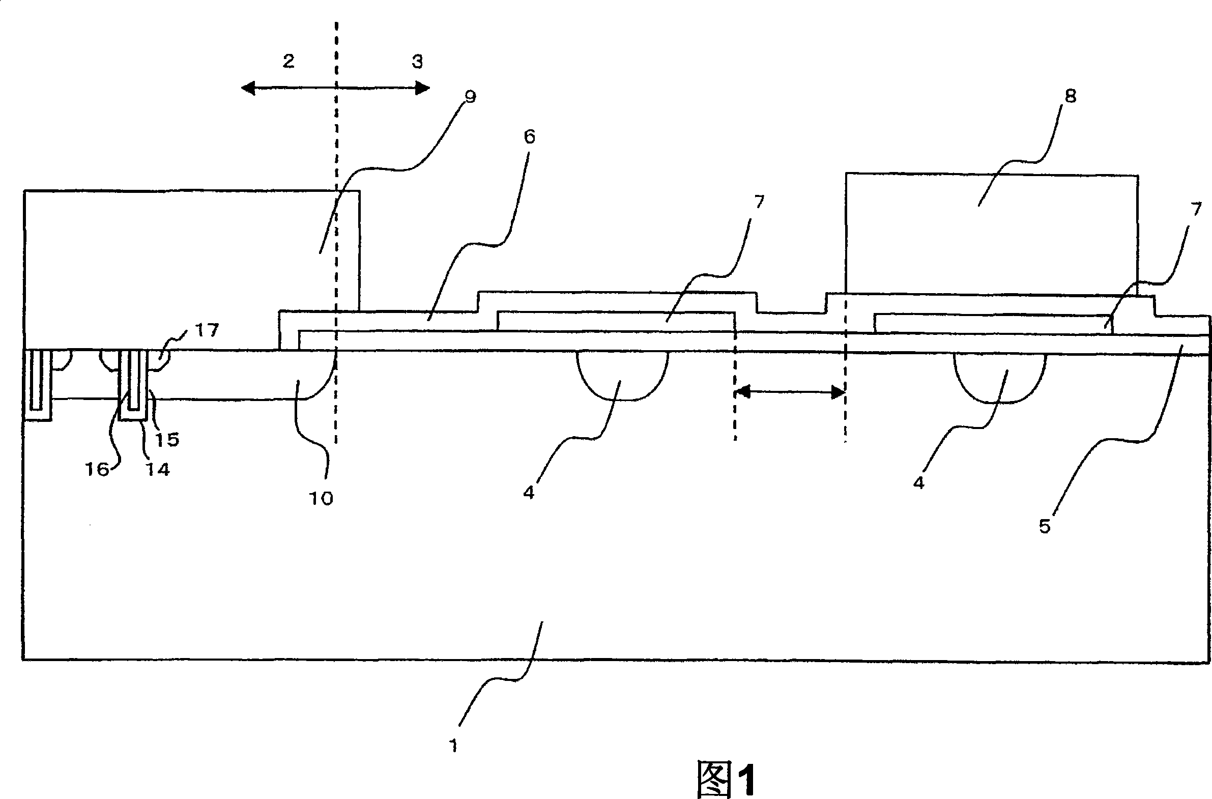
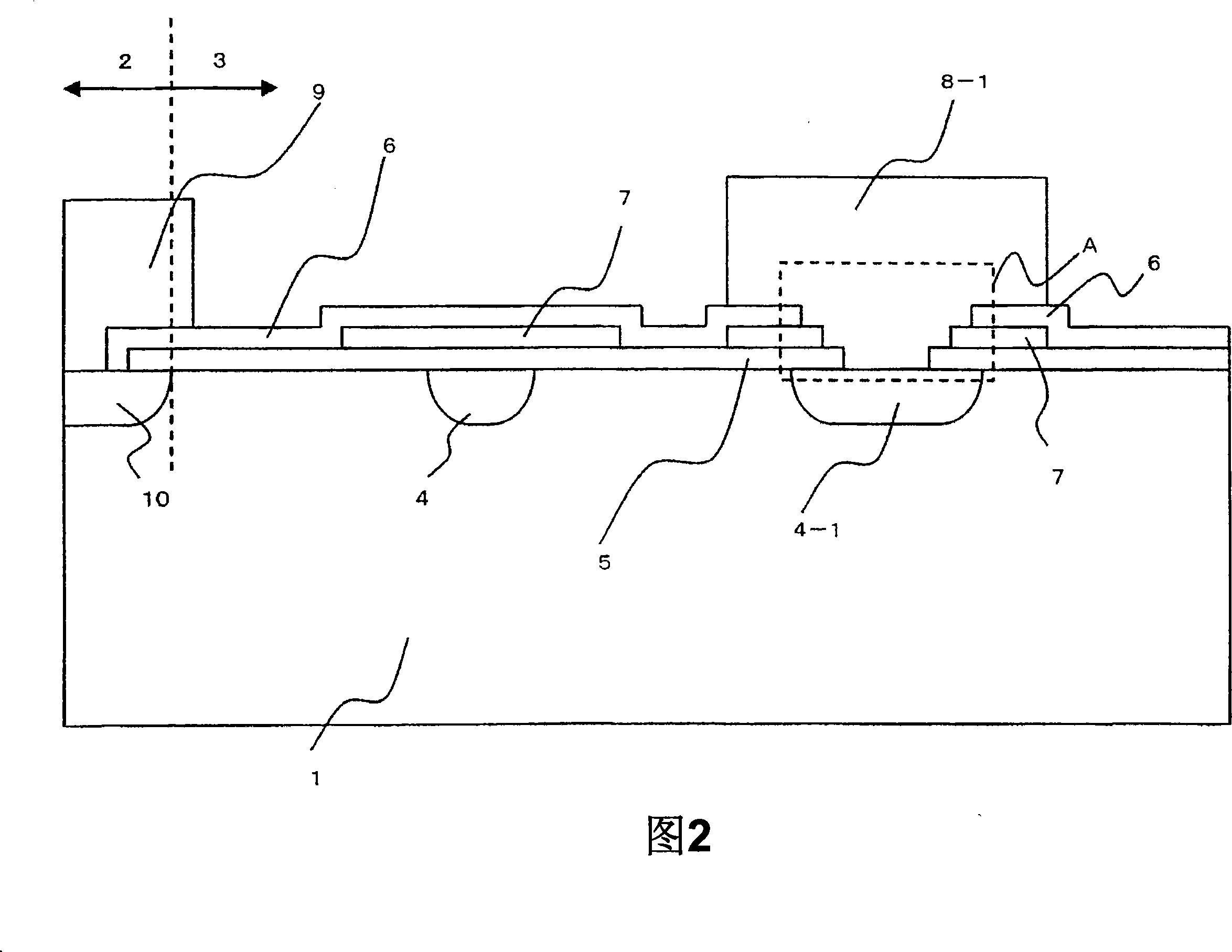
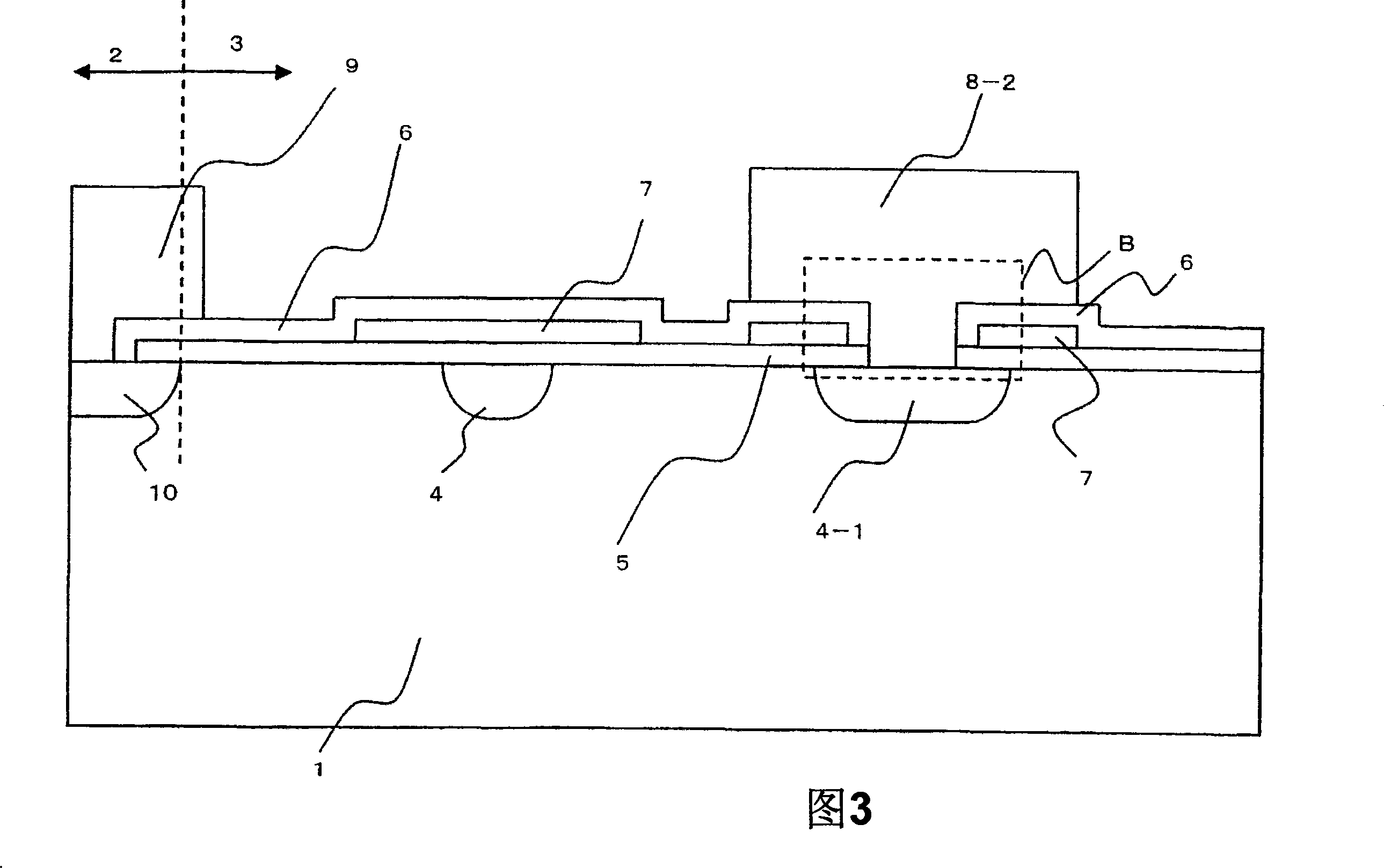
[0050] 1 to 4 are main part cross-sectional views of different edge termination structures of the power semiconductor device of the present invention. 5-1 to 5-3 are cross-sectional views of different edge termination structures in corner portions of the power semiconductor device of the present invention. 6 is an enlarged cross-sectional view of an edge termination structure in a corner portion of the power semiconductor device of the present invention. 7-1 to 7-4 are cross-sectional views taken along the line XX' of the edge termination structure of FIG. 5-1(b), which are used to illustrate the method of manufacturing the power semiconductor device of the present invention. Fig. 8 is a cross-sectional view taken along line Y-Y' of Fig. 5-1(b), showing the non-c...


PUM


Abstract

The present invention provides an electric power semiconductor device, including a field plate which uses thin metallic film in edge termination structure, and capable of allowing the width of the edge termination structure to reduce even though there is large profile etching quantity or changed etching quantity, and showing excellent reliability of forward direction breaking voltage ability for a long time, as well as minimizing the change of the forward direction breaking voltage ability. The edge termination structure includes a plurality of p type guard rings, first insulating films for covering the surfaces of a plurality of annular p type guard rings, and annular field plate setting on the top of the guard ring by the first insulating film. The field plate includes multicrystal silicon film and metallic film which thickness is more than that of the multicrystal silicon film. The guard ring includes a first guard ring and a second guard ring, the multicrystal silicon film is set on the first guard ring by the first insulating film, and a twolayer field plate composed of the multicrystal silicon film and the metallic film stacked by the second insulating films, is set on the second gurad ring, the first and the second guard rings are set alternately.

Description

technical field [0001] The present invention relates to power semiconductor devices used in power converters and the like. Background technique [0002] 9 shows a main part cross-sectional view of an active region 20 where a main current flows in the center of a conventional power semiconductor device and an edge termination structure 30 located on the periphery surrounding the active region 20 . The edge termination structure portion 30 is a portion provided to reliably maintain this OFF state voltage between the upper electrode and the lower electrode (the lower electrode is not shown) of the n-type semiconductor substrate 100 of the device in the OFF state. When the OFF-state voltage increases, the width of the edge termination structure portion 30 (the width of the edge termination structure portion 30 in the direction extending from the boundary of the active region 20 toward the outer edge of the semiconductor substrate 1 ) needs to be increased. However, as the width...

Claims


Application Information

Patent Timeline
IPC IPC(8): H01L29/06H01L29/78H01L29/739
Inventor 胁本博树大月正人椎木崇
Owner FUJI ELECTRIC CO LTD
Why Eureka
Try Eureka