

Test carrier plate
A technology for testing carrier boards and test pads, which is applied in electronic circuit testing, single semiconductor device testing, and electrical measurement, etc., can solve problems such as affecting accuracy, disconnection of wire 140, poor reliability, etc., to improve reliability and improve reliability. The effect of accuracy
- Summary
- Abstract
- Description
- Claims
- Application Information
AI Technical Summary
Problems solved by technology
Method used
Image

Examples
Embodiment Construction
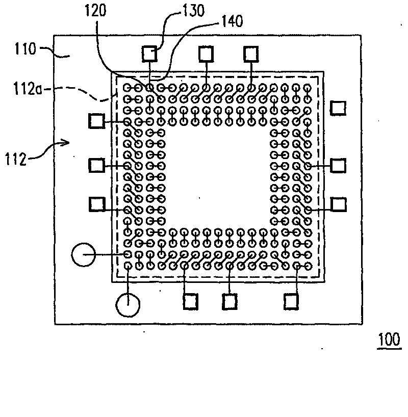
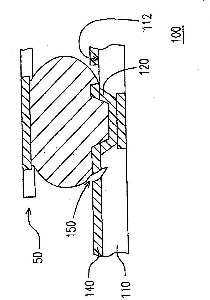
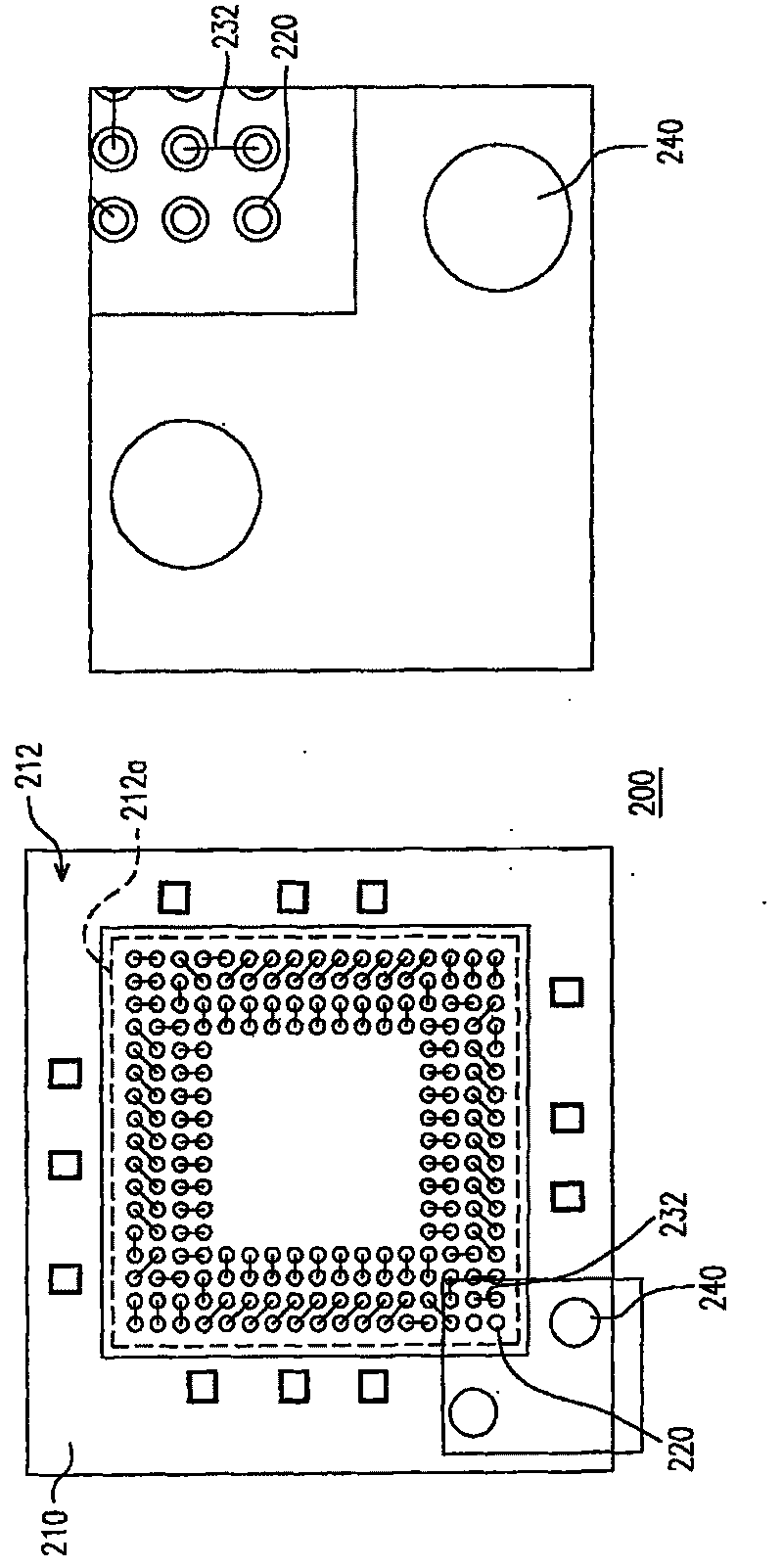
[0045] Figure 2A It is a top view of the test carrier board in an embodiment of the present invention, Figure 2B for Figure 2A A cross-sectional view of a mid-test carrier carrying a packaged component. Please refer to Figure 2A and Figure 2B , the test carrier 200 can be applied to test a packaged component 50, the test carrier 200 includes a dielectric layer 210, a plurality of pads 220, a pad connection line 232, a plurality of test pads 240 and a plurality of first wires 252 .
[0046] According to the above, the dielectric layer 210 has a first surface 212 and a second surface 214 opposite thereto, and the first surface 212 has a component bonding area 212 a for carrying the package component 50 . The pads 220 are arranged in an array, for example, and are located on the first surface 212 in the device bonding area 212 a for bonding with the package device 50 . The pad connection lines 232 are located on the first surface 212 and electrically connected to the p...
PUM
 Abstract
Description
Claims
Application Information