

Thin-film transistor array substrate and manufacturing method thereof
A technology for thin film transistors and array substrates, which is applied in the field of thin film transistor array substrates and thin film transistor array substrate manufacturing, can solve problems such as poor contact, residual dielectric layer, and panel performance deterioration, and achieve the effect of increasing the shading effect.
- Summary
- Abstract
- Description
- Claims
- Application Information
AI Technical Summary
Problems solved by technology
Method used
Image

Examples
no. 1 example
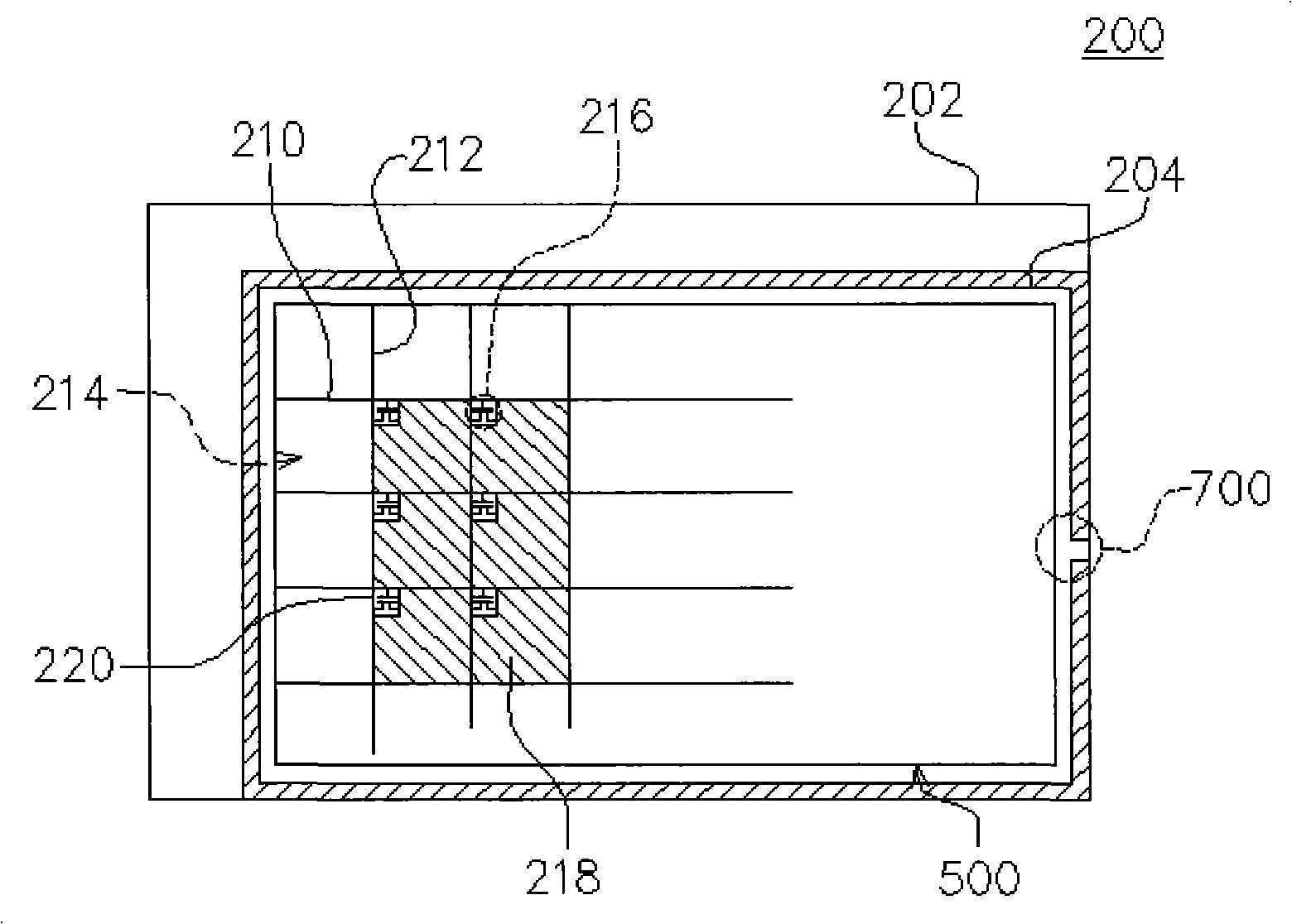
[0052] FIG. 2 is a schematic perspective view of a thin film transistor liquid crystal display panel according to the present invention.
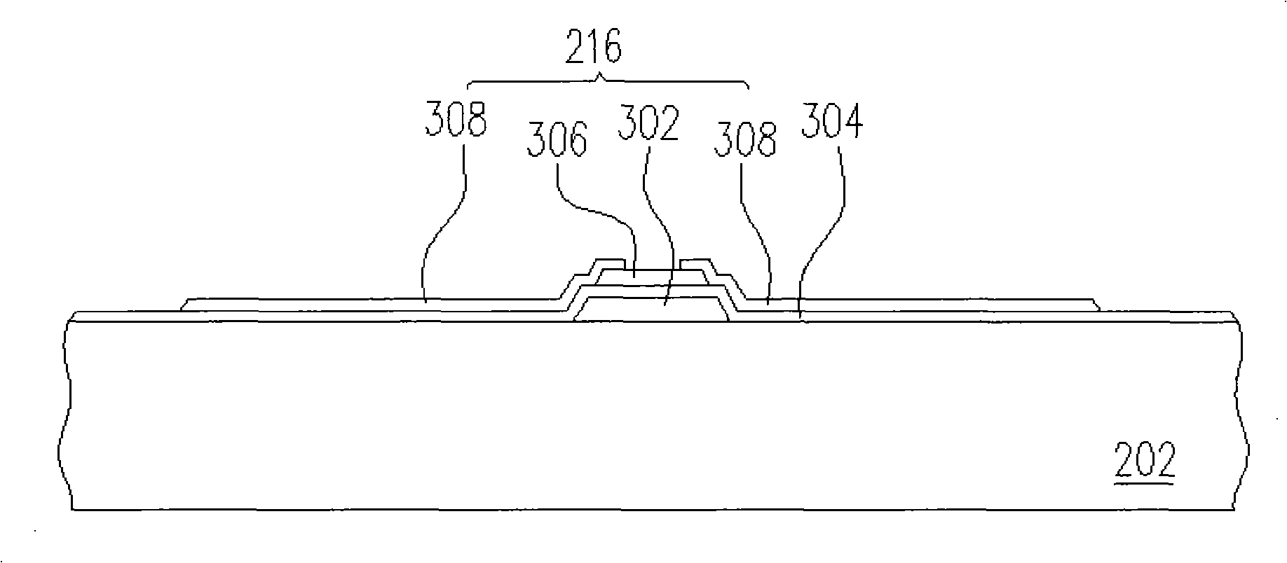
[0053] Please refer to FIG. 2, the thin film transistor liquid crystal display panel 200 of the present invention is composed of a thin film transistor array substrate 202, a counter substrate 204 and a liquid crystal layer (not shown), wherein the liquid crystal layer is located on the thin film transistor array substrate 202 and the opposite substrate 204 . On the TFT array substrate 202 there are several scanning wires 210 , several data wires 212 , TFTs 216 , pixel electrodes 218 , color filter films (not shown) and several color filter stacks 220 . The data wires 212 and the scan wires 210 form several pixel regions 214 . Furthermore, thin film transistors 216 are disposed at intersections of the data wires 212 and the scan wires 210 , and are controlled by the data wires 212 and the scan wires 210 . The pixel electrodes 218 are disp...
no. 2 example
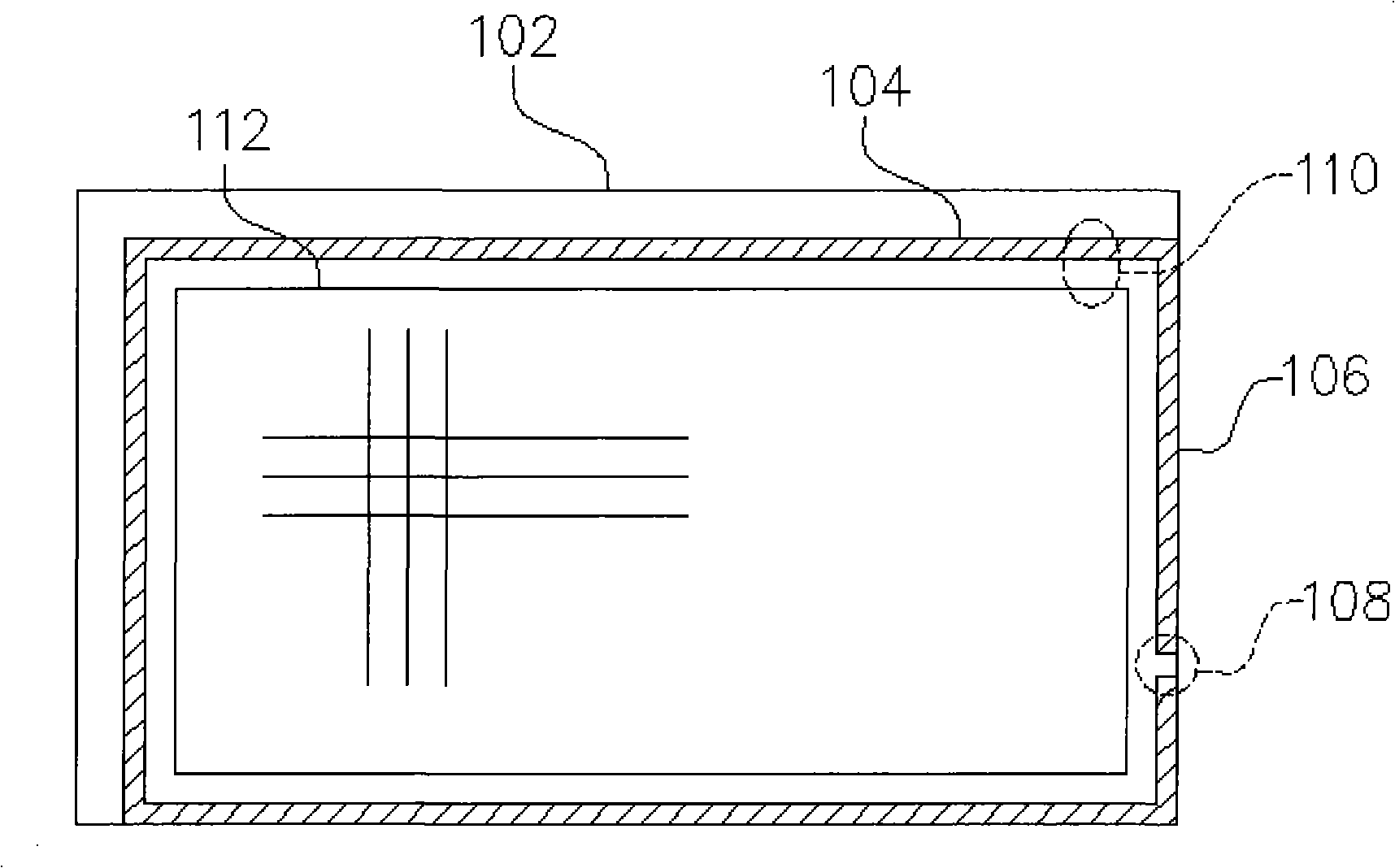
[0061] This embodiment is mainly aimed at improving the border of the display area of the thin film transistor liquid crystal display panel of the present invention, please refer to figure 2 The display area 500 refers to the area with the pixel area 214 that can display patterns and colors; on the contrary, the part outside the display area 500, that is, the edge of the display area is the "non-display area".
[0062] Figure 5A to Figure 5C According to a second embodiment of the present invention, a schematic cross-sectional view of the manufacturing process of a thin film transistor liquid crystal display panel, the difference between it and the first embodiment is as follows: Please refer to Figure 5A , the first metal layer formed and patterned on the substrate 202, except Figure 3A In addition to the components, there is a metal layer 502 formed on the edge of the display area 500 . Afterwards, a gate insulating layer 304 is formed on the substrate 202 , which is...
no. 3 example
[0069] This embodiment is mainly aimed at improving the liquid crystal injection hole (LC injection hole) at the edge of the display area of the thin film transistor liquid crystal display panel of the present invention, please refer to figure 2 The position of the liquid crystal injection port 700 is at the edge of the display area 500, from which liquid crystal can be injected.
[0070] Figure 7A to Figure 7B The schematic sectional view of the manufacturing process of the TFT-LCD panel according to the third embodiment of the present invention is substantially the same as that of the second embodiment, the difference lies in the steps after forming the adjacent or partially overlapping metal layers 502 and 506 . Please refer to Figure 7A , in order to facilitate the injection of liquid crystals, a larger aperture needs to be reserved in the liquid crystal injection port 700, so at this time, several color filter blocks can be formed on the substrate 202 exposed by the...
PUM
 Abstract
Description
Claims
Application Information