Reference current circuit

A technology of reference current and reference voltage, applied in the direction of adjusting electrical variables, control/regulating systems, instruments, etc., can solve the problems of low temperature dependence of resistance, reducing the temperature dependence of reference current, and limitation of adjustment range.

Inactive Publication Date: 2008-10-01
PANASONIC CORP
View PDF0 Cites 12 Cited by
  • Summary
  • Abstract
  • Description
  • Claims
  • Application Information

AI Technical Summary

Problems solved by technology

[0024] However, in recent years, in the field of semiconductor integrated circuits, with the miniaturization of resistors, the temperature dependence of resistance has become very low
Moreover, when adjusting ...

Method used


Image

  • Reference current circuit
  • Reference current circuit
  • Reference current circuit

Examples


no. 1 example

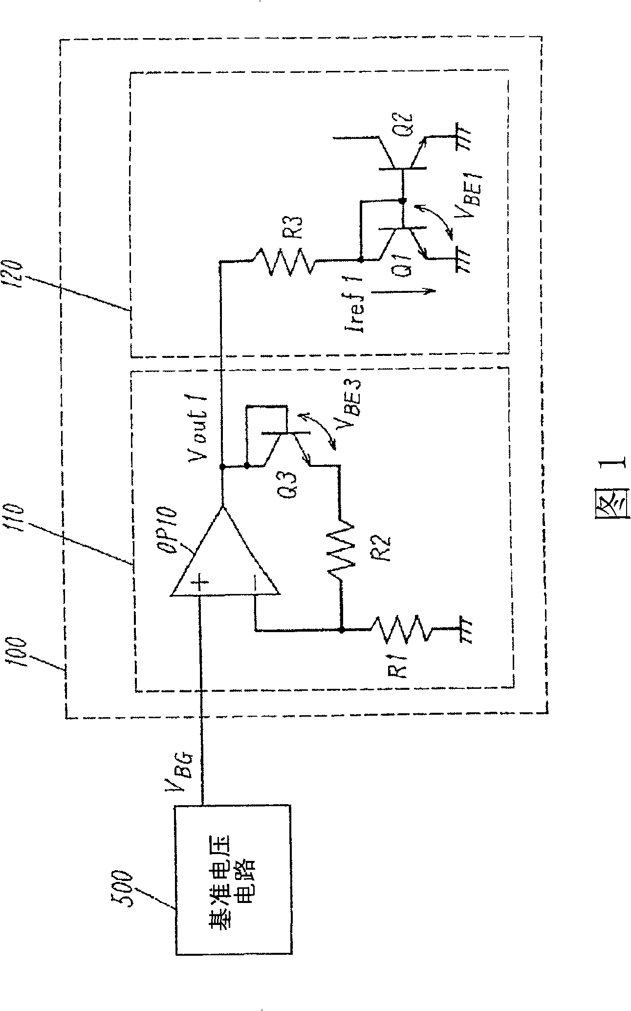
[0040] FIG. 1 shows the structure of a reference current circuit of a first embodiment of the present invention.

[0041] The reference current circuit 100 includes a non-inverting amplifier circuit 110 and a current source circuit 120 receiving an input from the non-inverting amplifier circuit 110 .

[0042] The non-inverting amplifier circuit 110 is composed of an amplifier circuit OP10, a resistor R1, a resistor R2, and a transistor Q3. The amplifier circuit OP10 has an inverting input terminal, a non-inverting input terminal, and an output terminal; a resistor R1 is inserted into the wiring to connect the inverting input terminal and a ground terminal; a resistor R2 and a transistor Q3 functioning as a temperature compensation element are inserted into the wiring Connect the output terminal and inverting input terminal. The non-inverting input terminal of the amplifier circuit OP10 receives a reference voltage V that does not depend on the temperature T and the power supp...

no. 2 example

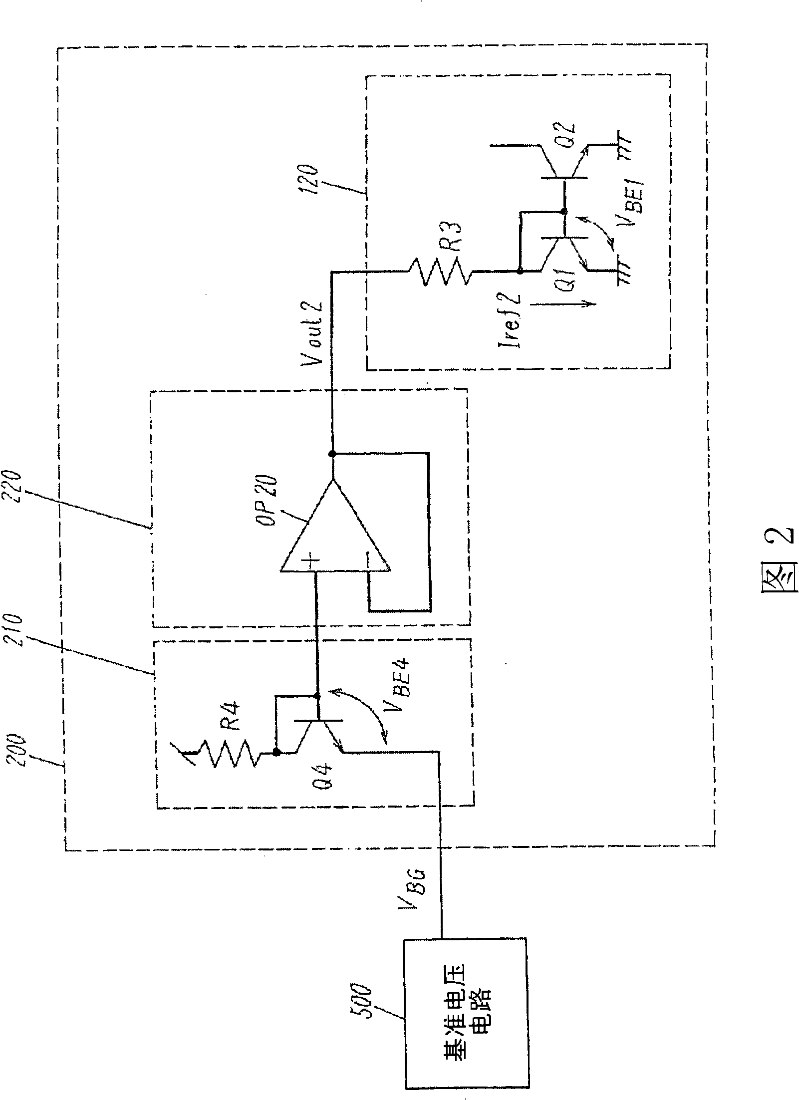
[0071] FIG. 2 shows the structure of a reference current circuit of a second embodiment of the present invention.

[0072] The reference current circuit 200 includes a temperature compensation circuit 210 , a voltage follower 220 receiving an output of the temperature compensation circuit 210 as an input, and a current source circuit 120 receiving an output of the voltage follower 220 as an input.

[0073] The temperature compensation circuit 210 is composed of a transistor Q4 and a resistor R4. Transistor Q4 receives the reference voltage V from its emitter BG input, the collector and base of transistor Q4 are connected to each other. Resistor R4 is inserted into the wiring connecting the power supply terminal and the collector of transistor Q4.

[0074] The voltage follower 220 is constituted by an amplifier circuit OP20 including an inverting input terminal, a non-inverting output terminal, and an output terminal. The collector and base of the transistor Q4 are connected...

no. 3 example

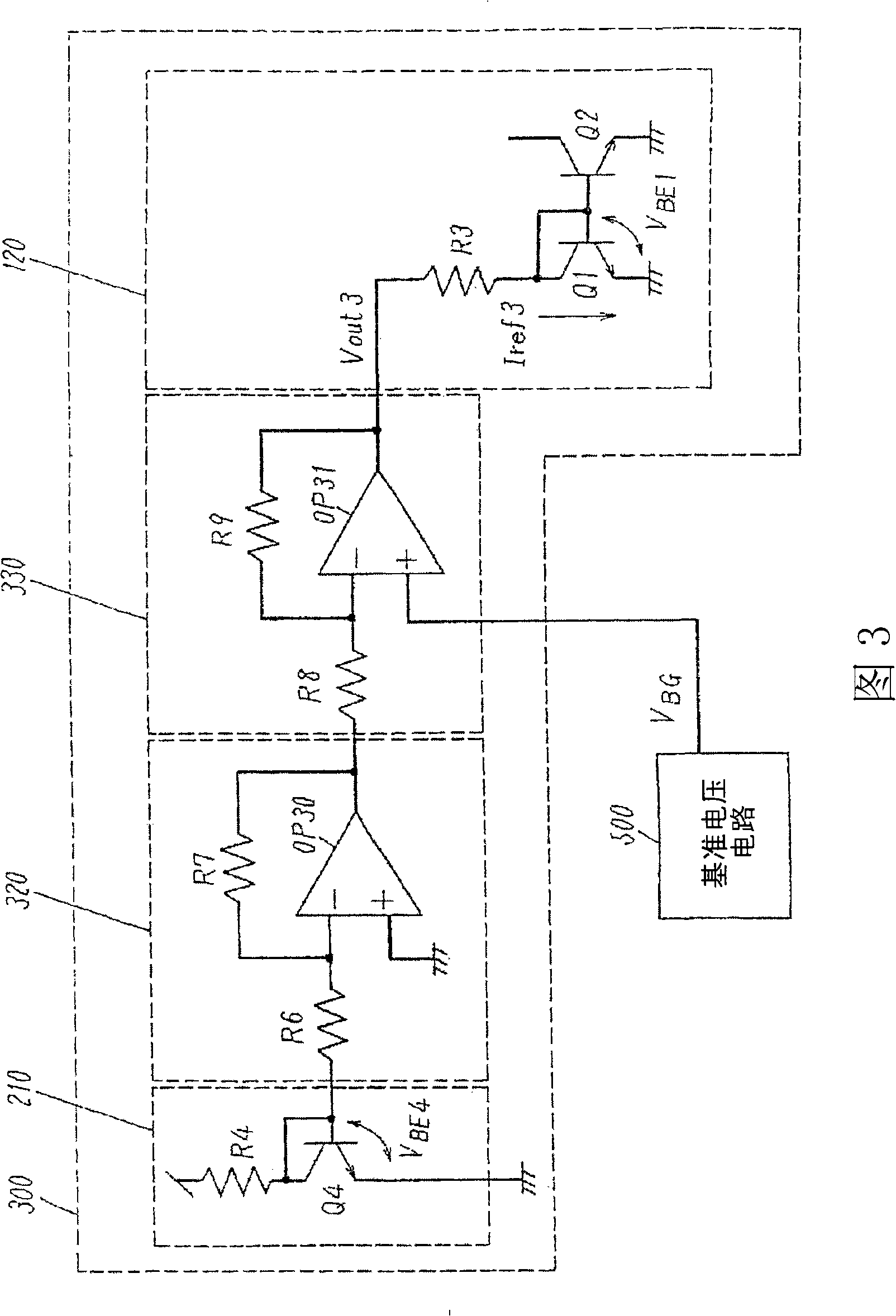
[0099] FIG. 3 shows the structure of a reference current circuit of a third embodiment of the present invention.

[0100] The reference current circuit 300 includes a temperature compensation circuit 210 , an inverting amplifier circuit 320 , an inverting amplifier circuit 330 and a current source circuit 120 . The inverting amplifier circuit 320 receives the output of the temperature compensation circuit 210 as an input; the inverting amplifier circuit 330 receives the output of the inverting amplifier circuit 320 as an input; the current source circuit 120 receives the output of the inverting amplifier circuit 320 as an input.

[0101] The temperature compensation circuit 210 is composed of a transistor Q4 and a resistor R4. The emitter of the transistor Q4 is grounded, and the collector and base of the transistor Q4 are connected to each other. Resistor R4 is inserted into the wiring connecting the power supply terminal and the collector of transistor Q4.

[0102] The inv...


PUM


Abstract

The invention provides a reference current circuit which can reduce temperature dependency of reference current even though in the situation of using a resistor of a resistance provided with very low temperature dependency. The reference current circuit comprises: a reference voltage V receiving temperature compensation and a noninverting amplifier circuit 110 generating a voltage V on an output point; a current source circuit 120 consisted of a transistor Q1 which is connected to the output point via the resistor and a transistor Q2 which receives a voltage equal to a voltage V generated among terminals of Q1 and generating related circuit. The circuit 110 (i) comprises: a third transistor Q3. A voltage V generated among the terminals of the Q3 is provided with the same temperature property with V, and is structured to make V is the sum of (a) a temperature compensation voltage component based on the reference voltage V and (b) a voltage component equal to the voltage V.

Description

technical field [0001] The present invention relates to a reference current circuit for generating a bias current supplied to an analog circuit. Background technique [0002] FIG. 4 shows the structure of a conventional reference current circuit. [0003] The reference current circuit 400 includes a non-inverting amplifier circuit 410 and a current source circuit 120 . [0004] The non-inverting amplifier circuit 410 is composed of an amplifier circuit OP40, a resistor R1, and a resistor R2. The amplifier circuit OP40 includes an inverting input terminal, a non-inverting input terminal and an output terminal; a resistor R1 is inserted into the wiring to connect the inverting input terminal and the ground terminal; a resistor R2 is inserted into the wiring to connect the output terminal and the inverting input terminal. The non-inverting input terminal of the amplifier circuit OP40 receives the reference voltage Vdd which does not depend on the temperature T and the power s...

Claims


Application Information

Patent Timeline
IPC IPC(8): G05F3/16
Inventor 井上敦雄松野则昭
Owner PANASONIC CORP
Why Eureka
Try Eureka