Radiating unit and semiconductor package having the same

A heat dissipation unit and package technology, applied in semiconductor devices, semiconductor/solid-state device parts, electrical components, etc., can solve problems such as uneven flat parts, crushing chip 12 circuits, etc.

Inactive Publication Date: 2008-10-15
SILICONWARE PRECISION IND CO LTD
View PDF5 Cites 2 Cited by
  • Summary
  • Abstract
  • Description
  • Claims
  • Application Information

AI Technical Summary

Problems solved by technology

[0008] see Figure 1B and Figure 1C , the heat dissipation unit is made by stamping, and the corner end of the stamped product is prone to protruding deformation due to the extrusion between materials and the stress cannot be released, and this protruding deformation occurs in the flat part 130 and the adjacent extended portion 131 will cause unevenness in the flat portion, and when the heat dissipation unit 13 is attached and combined on the chip 12, the protruding corner end will produce a contact point with the chip 12, and mold pressing During the process, the pressure will be concentrated on the contact point and then crush the circuit on the chip 12

Method used


Image

  • Radiating unit and semiconductor package having the same
  • Radiating unit and semiconductor package having the same
  • Radiating unit and semiconductor package having the same

Examples


no. 1 example

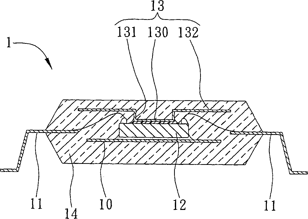
[0047] Please refer to Figure 2A to Figure 2D , is a schematic diagram showing the first embodiment of the heat dissipation unit and the semiconductor package of the present invention.

[0048] Please refer to FIG. 2A , an electronic component 21 is placed and electrically connected on the carrier 20 to form a package semi-finished product, wherein the carrier 20 can be a substrate or a lead frame, and the electronic component 21 generates high heat during operation. The chips are electrically connected to the carrier 20 by bonding wires.

[0049] Please refer to FIG. 2B, the central area of ​​the electronic component 21 can be connected with a heat dissipation unit 22, the heat dissipation unit 22 includes a flat part 220 attached to the top of the electronic component 21, connected to the side of the flat part 220 and facing An extension 221 extending away from the electronic component 21, and a heat dissipation portion 222 connected to the extension 221 and extending outw...

no. 2 example

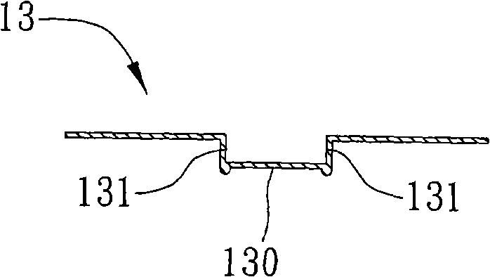
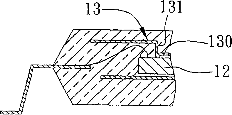
[0058] see Figure 3A and Figure 3B , is a three-dimensional schematic diagram showing the second embodiment of the heat dissipation unit of the present invention. This embodiment is substantially the same as the previous embodiment, but the difference is that the stress relief part 223 of this embodiment is a mausoleum located at the junction of any two extension parts 221 The line extends to the strip-shaped slot at the corner end of the mausoleum line to prevent the stress from concentrating on the mausoleum line and deform the mausoleum line, so as to ensure that the flat portion 220 of the heat dissipation unit 22 remains flat.

[0059] Compared with the prior art where the chip is electrically connected to the substrate by wire bonding, a heat transfer element must be used to connect the heat sink exposed to the encapsulant, which increases the cost of the manufacturing process and may damage the chip during the molding process. Risk, the heat dissipation unit 22 of th...


PUM


Abstract

The invention discloses a radiating unit and a semiconductor encapsulating part provided with the radiating unit, wherein, the semiconductor encapsulating part comprises a bearing part, an electronic component electrically connected to the bearing part, a flat part attached to and combined with the electronic component, an extension part connected to the flat part, the radiating unit of a radiating part connected to the extension part, and a molding colloid used for encapsulating the electronic component and the radiating unit; wherein, at least the angle end of the border crest line of the extension part and the flat part is provided with a stress release part to remove the convex angle end of the radiating units caused by stress concentration in the punching process so as to maintain the flatness of the flat part, thus preventing the circuit on the electronic component from being pressed and damaged by a contact point generated between the flat part and the electronic component in the mould pressing process.

Description

technical field [0001] The invention relates to a semiconductor package technology, more specifically, to a heat dissipation unit and a semiconductor package with the heat dissipation unit. Background technique [0002] Semiconductor chips generate high heat during operation. Therefore, in the manufacturing process of semiconductor packages today, a heat sink or heat dissipation structure is connected to the semiconductor chip to improve heat dissipation efficiency. [0003] U.S. Patent No. 6,444,498 discloses a manufacturing method of a semiconductor package, which mainly provides a substrate carrying a plurality of chips arranged in an array, and connects a large-area heat sink on the upper surface of each chip, and then performs Package molding, singulation, and removal of encapsulant above the top surface of the heat sink. However, the above manufacturing method will inevitably cut the heat sink during the singulation process, and the encapsulant remaining on the heat s...

Claims


Application Information

Patent Timeline
Patent Type & Authority Applications(China)
IPC IPC(8): H01L23/367H01L23/488H01L23/31
CPCH01L2224/48247H01L2224/48091H01L2224/32245H01L2924/0002H01L2224/73265H01L2924/00014H01L2924/00
Inventor 赖正渊黄建屏黄致明王愉博萧承旭
Owner SILICONWARE PRECISION IND CO LTD
Why Eureka
Try Eureka