Semiconductor package, method of fabricating the same and semiconductor package module for image sensor

A technology of semiconductor and sealant, which is applied in the direction of semiconductor devices, semiconductor/solid-state device components, electric solid-state devices, etc., can solve the problems that it is difficult to manufacture light enough and simple plastic packages, and the structure of plastic packages is complex, so as to achieve simple configuration, The effect of low production cost

Inactive Publication Date: 2008-10-29
崔显圭 +1
View PDF0 Cites 13 Cited by
  • Summary
  • Abstract
  • Description
  • Claims
  • Application Information

AI Technical Summary

Problems solved by technology

[0009] [09] Similar to ceramic packages, plastic packages are also structurally complex, so it is difficult to manufacture plastic packages that are light enough and simple

Method used


Image

  • Semiconductor package, method of fabricating the same and semiconductor package module for image sensor
  • Semiconductor package, method of fabricating the same and semiconductor package module for image sensor
  • Semiconductor package, method of fabricating the same and semiconductor package module for image sensor

Examples


Embodiment Construction

[0063] [60] Exemplary embodiments of the present invention will be described in more detail below with reference to the accompanying drawings. However, the invention may be embodied in different forms and should not be construed as limited to the described embodiments of the invention. Rather, these embodiments are provided so that this disclosure will be thorough and complete, and will fully convey the scope of the invention to those skilled in the art. In the drawings, the thickness of layers and regions are exaggerated for clarity. It will also be understood that when a layer is referred to as being "on" another layer or substrate, it can be directly on the other layer or substrate, or intervening other layers may be present. The same reference numbers are used throughout the specification to refer to the same elements.

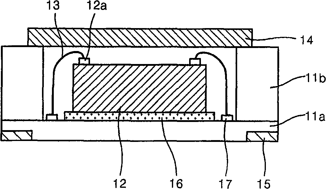
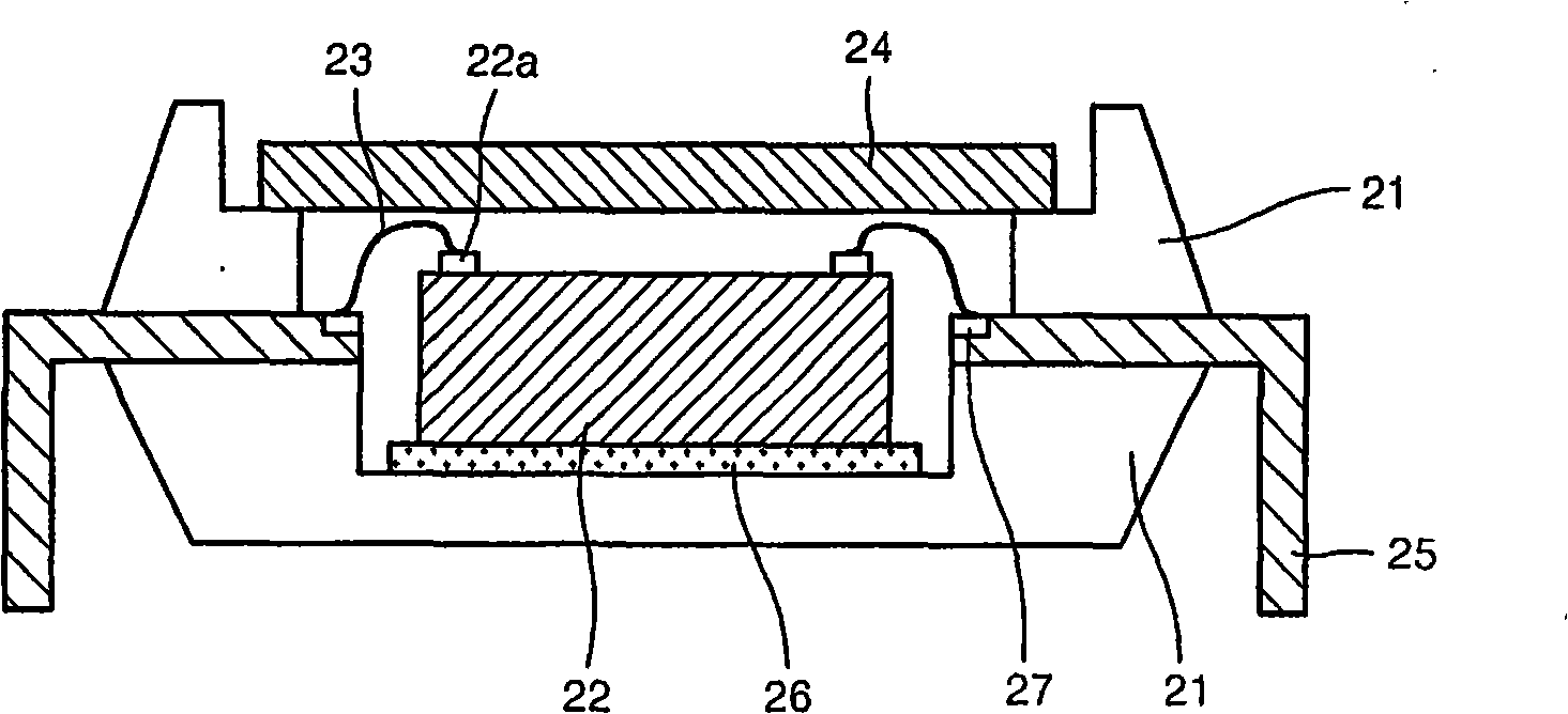
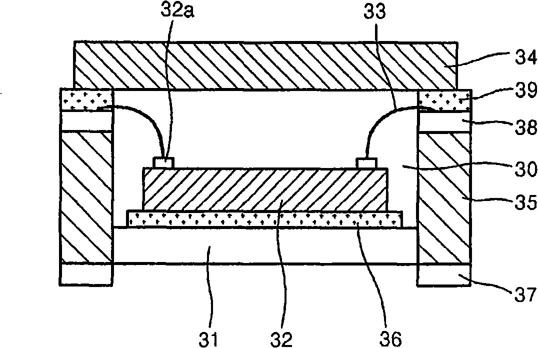
[0064] [61] FIGS. 3A to 3C are a cross-sectional view, a plan view, and a bottom view, respectively, of a semiconductor package for an image sensor acco...


PUM


Abstract

Provided are a semiconductor package, a method of fabricating the same, and a semiconductor package module for an image sensor. The semiconductor package includes a mounting portion on which a semiconductor chip is mounted; a semiconductor chip including a plurality of bonding pads disposed along an edge thereof, wherein the semiconductor chip adhered onto the mounting portion; a plurality of leads spaced apart from a sidewall of the semiconductor chip and having a greater height than the semiconductor chip; an encapsulant for fixing the mounting portion and the leads and encapsulating a bottom surface and a sidewall of the semiconductor package and exposing top and bottom surfaces of the leads; bonding wires for connecting the bonding pads of the semiconductor chip with the exposed top surfaces of the leads; and a transparent plate adhered onto the leads a predetermined space apart from the semiconductor chip.

Description

technical field [0001] [01] The present invention relates to a semiconductor package, and more particularly, to a semiconductor package including a semiconductor chip of an image sensor, a method of manufacturing the semiconductor package, and a semiconductor package module for an image sensor. Background technique [0002] [02] A semiconductor package including a CMOS image sensor (CIS) has been widely used in a mobile phone camera or a charge-coupled device, which has developed rapidly in recent years. Due to the increasing consumer demand for high-performance, light-weight and simple configurations, many researchers have worked to develop semiconductor packages that can be used in chip-scale packages (CSPs) for mounting semiconductor packages on printed circuit boards (PCBs). [0003] [03] Traditionally, ceramic packages and plastic packages have been used as CSPs for image sensors. [0004] [04] FIG. 1 is a cross-sectional view of a conventional ceramic package for an i...

Claims


Application Information

Patent Timeline
Patent Type & Authority Applications(China)
IPC IPC(8): H01L27/146
CPCH01L2224/49175H01L24/97H01L2224/48091H01L2924/0002H01L2224/73265H01L2224/48247H01L2924/18165H01L2224/92247H01L2224/05553H01L2924/16195H01L2924/00014H01L2924/00H01L23/02H01L27/146
Inventor 崔显圭高楚峰
Owner 崔显圭
Why Eureka
Try Eureka