Probe card and method for fabricating the same

A probe card and probe module technology, used in electronic circuit testing, instrumentation, electrical measurement, etc., can solve problems such as time-consuming, deteriorating block alignment, and increasing block length.

Active Publication Date: 2008-11-12
AMST CO LTD
View PDF2 Cites 10 Cited by
  • Summary
  • Abstract
  • Description
  • Claims
  • Application Information

AI Technical Summary

Problems solved by technology

However, as the area to be tested increases, the number of squares and the length of squares to be precisely aligned also increase
Therefore, there is a problem that it takes a lot of time to precisely align the blocks, and the alignment of the blocks may deteriorate during testing

Method used


Image

  • Probe card and method for fabricating the same
  • Probe card and method for fabricating the same
  • Probe card and method for fabricating the same

Examples


Embodiment Construction

[0025] Reference will now be made in detail with reference to embodiments, examples of which are illustrated in the accompanying drawings. Wherever possible, the same reference numbers will be used throughout the drawings to refer to the same or like parts.

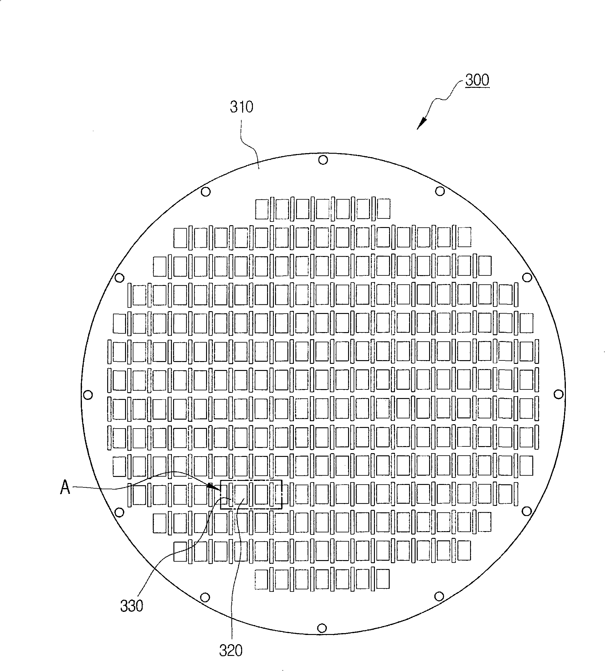
[0026] Hereinafter, a probe card and a method of manufacturing the same according to one general embodiment will be described in detail with reference to the accompanying drawings. image 3 is a plan view of a probe card according to an embodiment of the present invention. Figure 4 is image 3 An enlarged plan view of part A of . Fig. 5 is a cross-sectional view taken along line B-B' of Fig. 4 . FIG. 6 is a perspective view of FIG. 4 . Figure 7 is an isolated perspective view of FIG. 6 . Figure 8 is an enlarged view of part C of FIG. 6 . Figure 9 is a plan view of a printed circuit board positioned sideways. as well as, Figure 10 is a plan view of a lower surface printed circuit board according to a general em...


PUM


Abstract

The present disclosure relates to a probe card for testing semiconductor chips on a semiconductor wafer comprising: a circuit board receiving electrical signals from outside; a plurality of unit probe modules contacting the semiconductor chips on the wafer to transfer the electrical signals; a space transformer having the plurality of probe modules seated on the upper portion thereof and electrically connected to the circuit board, wherein the respective probe modules are arranged at intervals from each other on the space transformer and the space transformer has vertical apertures penetrating through it up and down;and at least one vertical conductive medium electrically connecting the respective unit probe modules and the circuit board, wherein the vertical conductive medium is arranged in the vertical apertures provided in the space transformer and the respective unit probe modules are arranged at positions spaced from the vertical conductive medium.

Description

[0001] This application claims the benefit of Korean Patent Application No. 10-2007-0046099 filed May 11, 2007, the entire contents of which are hereby incorporated by reference. [0002] This application claims the benefit of Korean Patent Application No. 10-2007-0088270 filed on Aug. 31, 2007, the entire contents of which are hereby incorporated by reference. technical field [0003] The present invention relates to a probe card and its manufacturing method, and more particularly, to a method that can minimize process defects and improve Probe card for heat distortion, flatness and alignment accuracy and manufacturing method thereof. Background technique [0004] Generally, processes for manufacturing semiconductors are mainly classified into front-end processes and back-end processes. The front-end process, which is a manufacturing process, is a process for forming integrated circuit patterns on a wafer. The back-end process, which is an assembly process, is used to pro...

Claims


Application Information

Patent Timeline
Patent Type & Authority Applications(China)
IPC IPC(8): G01R1/073G01R31/26G01R31/28H01L21/66
CPCG01R1/07342Y10T29/49117G01R1/07378G01R1/06727H01L22/00
Inventor 郑仁范
Owner AMST CO LTD
Why Eureka
Try Eureka