Plasma semi-additive process method for manufacturing pcb

A circuit substrate and plasma technology, which is applied in the fields of printed circuit manufacturing, printed circuit, printed circuit secondary treatment, etc., can solve the problems of high developing failure rate and decreased adhesion of plating, etc., and achieve the effect of minimizing process failure

Inactive Publication Date: 2010-09-01
株式会社第4纪韩国
View PDF3 Cites 0 Cited by
  • Summary
  • Abstract
  • Description
  • Claims
  • Application Information

AI Technical Summary

Problems solved by technology

Also, after exposing and developing the dry film, that is, DFR, after making the DFR pattern wall, it will look like figure 1 In that way, the residue is left in the form of a line (line) for a long time, and the poor rate of development is very high. When copper plating is performed between the walls of the DFR pattern, there will be foreign matter and other plating defects between the patterns. The problem is that the adhesion of the plating is partially reduced due to interference or the hydrophobicity of the DFR pattern material itself.

Method used


Image

  • Plasma semi-additive process method for manufacturing pcb
  • Plasma semi-additive process method for manufacturing pcb
  • Plasma semi-additive process method for manufacturing pcb

Examples


Embodiment Construction

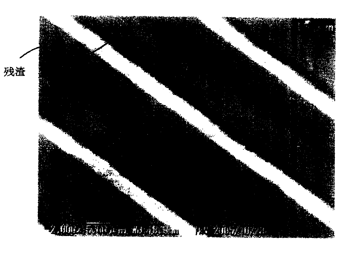
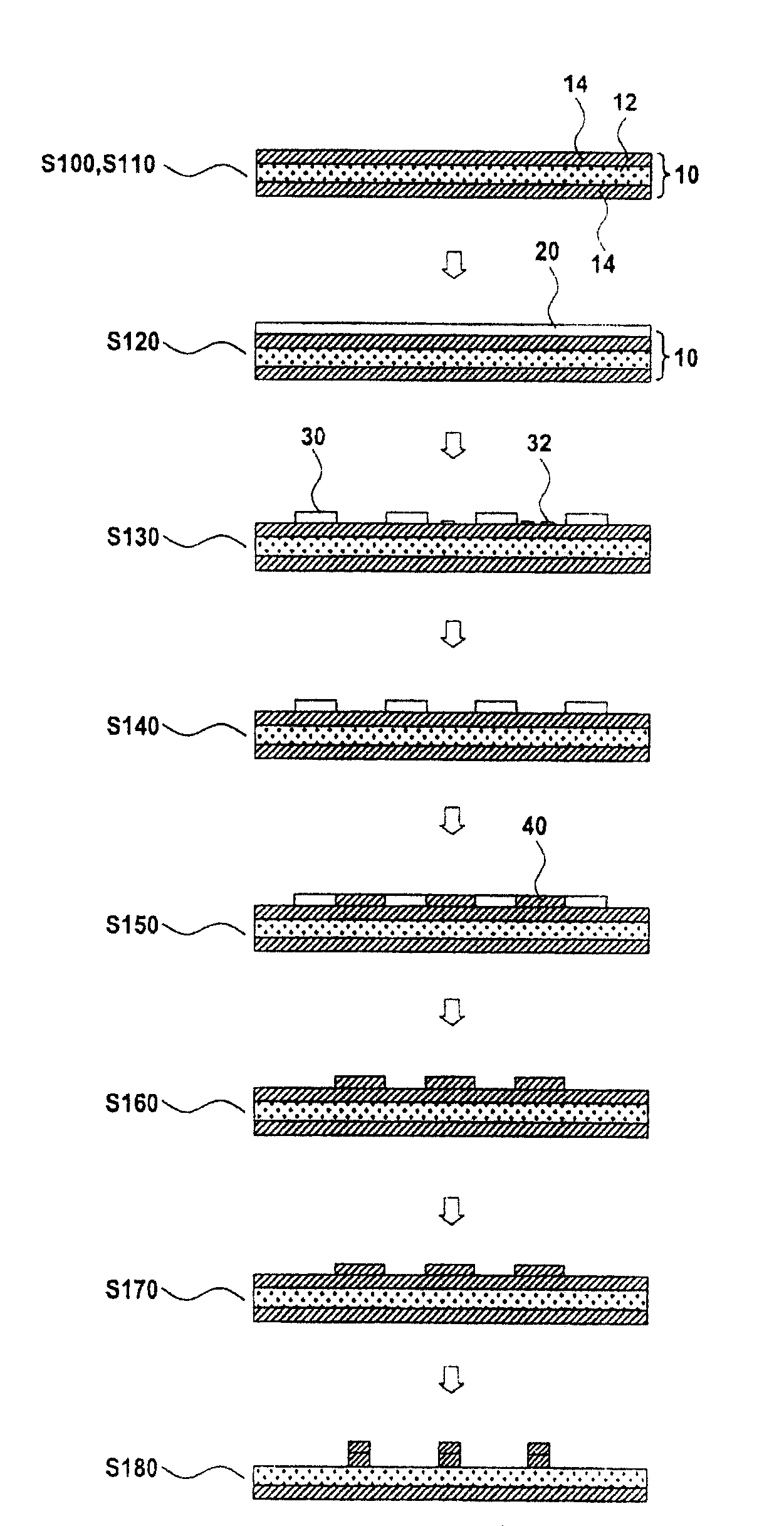
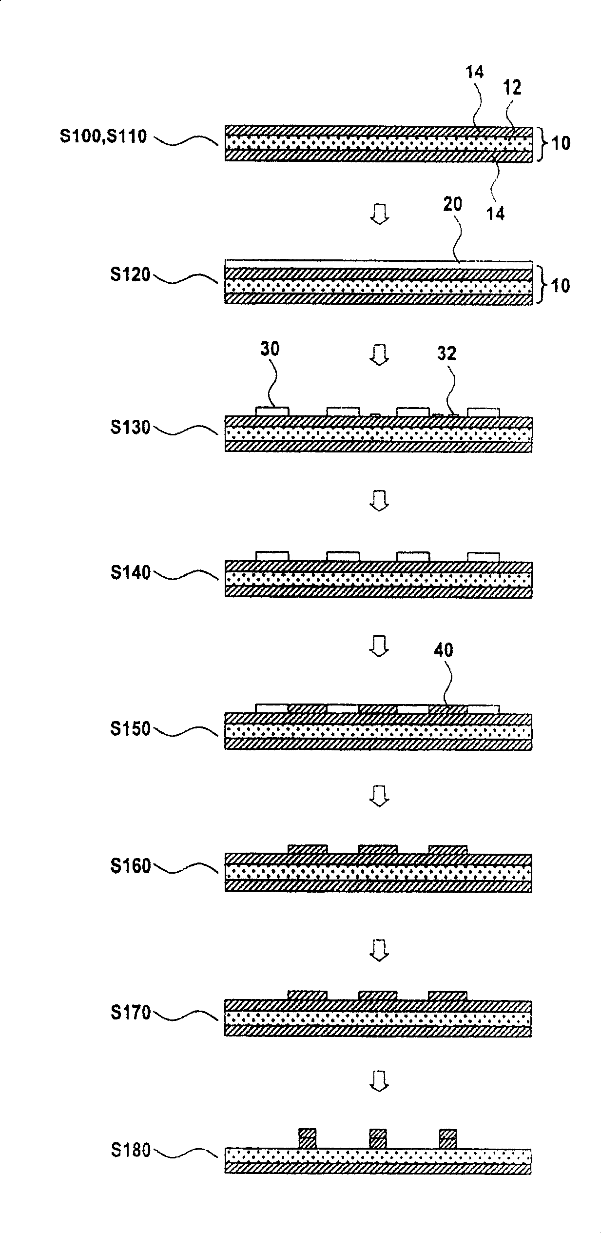
[0023] Hereinafter, preferred embodiments of the present invention will be described in more detail with reference to the drawings. figure 2 is a process diagram showing the PSAP method according to the present invention.

[0024] like figure 2 As shown, the PSAP process for manufacturing the printed circuit board involved in the present invention roughly includes a base substrate preparation stage (S100), a first plasma treatment stage (S110), and photoresist (photo resist) formation. stage (S120), pattern forming stage (S130), second plasma processing stage (S140), line forming stage (S150), first etching stage (S160), third plasma processing stage (S170) and second etching stage (S180).

[0025] In the base substrate preparation step ( S100 ), a double sided copper clad laminated board (double sided copper clad laminated: CCL) ( 10 ) is used as the base substrate.

[0026] The above-mentioned laminate (CCL) (10) has copper foil on both surfaces of the plate-shaped subs...


PUM


Abstract

Disclosed herein is a method of manufacturing a printed circuit board using a plasma semi-additive process (PSAP), including: a first plasma-treating step of improving the adhesion of a DFR; a second plasma-treating step of performing descumming and surface-reforming by plasma-treating the surface between pattern walls formed after the first plasma-treating step; a third plasma- treating step of performing descumming and surface-reforming by forming a circuit by plating copper between the plasma-treated pattern walls, removing the pattern walls through a first etching step while copper remains on the substrate, and then plasma-treating the surface of the exposed substrate and the copper- plated surface; and a second etching step of completing an electric circuit by finally etching the plasma-treated substrate.

Description

technical field [0001] The present invention relates to a PSAP (Plasma Semi Additive Process, plasma semi-additive) method for the manufacture of printed circuit boards, and in particular to cleaning the printed circuit boards with plasma during the execution of the SAP (Semi Additive Process, semi-additive) process. Cleaning, etching (etching) and surface modification, thereby improving the adhesion between the micro-circuit pattern (pattern) and the base (base) substrate, and manufacturing higher-grade printed circuit boards. PSAP method for printed circuit board manufacturing. Background technique [0002] Generally speaking, a printed circuit board (PCB) refers to a thin plate on which electrical components such as integrated circuits, resistors, or switches are mounted. After the copper foil (Copper Foil) is pasted on the finished substrate, then the resist is printed on the wiring where the copper foil must be left, and the printed substrate is placed in an etchant tha...

Claims


Application Information

Patent Timeline
Patent Type & Authority Patents(China)
IPC IPC(8): H05K3/38H05K3/02
CPCH05K2203/1476H05K2203/095H05K3/382H05K3/108H05K3/06
Inventor 白泰逸
Owner 株式会社第4纪韩国
Why Eureka
Try Eureka